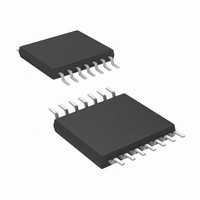
AT89LP214-20XU Atmel, AT89LP214-20XU Datasheet - Page 64

AT89LP214-20XU
Manufacturer Part Number
AT89LP214-20XU
Description
MCU 8051 2K FLASH 20MHZ 14-TSSOP
Manufacturer
Atmel
Series
89LPr
Datasheet
1.AT89LP213-20PU.pdf
(98 pages)
Specifications of AT89LP214-20XU
Core Processor
8051
Core Size
8-Bit
Speed
20MHz
Connectivity
SPI, UART/USART
Peripherals
Brown-out Detect/Reset, POR, PWM, WDT
Number Of I /o
12
Program Memory Size
2KB (2K x 8)
Program Memory Type
FLASH
Ram Size
128 x 8
Voltage - Supply (vcc/vdd)
2.4 V ~ 5.5 V
Oscillator Type
Internal
Operating Temperature
-40°C ~ 85°C
Package / Case
14-TSSOP
Package
14TSSOP
Device Core
8051
Family Name
AT89
Maximum Speed
20 MHz
Operating Supply Voltage
2.5|3.3|5 V
Data Bus Width
8 Bit
Number Of Programmable I/os
12
Interface Type
SPI/UART
Number Of Timers
2
Core
8051
Processor Series
AT89x
Maximum Clock Frequency
20 MHz
Data Ram Size
128 B
Mounting Style
SMD/SMT
Height
1.05 mm
Length
5.1 mm
Maximum Operating Temperature
+ 85 C
Minimum Operating Temperature
- 40 C
Supply Voltage (max)
5.5 V
Supply Voltage (min)
2.4 V
Width
4.5 mm
Lead Free Status / RoHS Status
Lead free / RoHS Compliant
Eeprom Size
-
Data Converters
-
Lead Free Status / Rohs Status
Details
22. On-chip Debug System
22.1
64
Physical Interface
AT89LP213/214
The AT89LP213/214 On-chip Debug (OCD) System uses a two-wire serial interface to control
program flow; read, modify, and write the system state; and program the nonvolatile memory.
The OCD System has the following features:
The On-chip Debug System uses a two-wire synchronous serial interface to establish communi-
cation between the target device and the controlling emulator system. The OCD interface is
controlled by two User Fuses. OCD is enabled by clearing the OCD Enable Fuse. When OCD is
enabled, the RST port pin is configured as an input for the Debug Clock (DCL). Either the XTAL1
or XTAL2 pin is configured as a bi-directional data line for the Debug Data (DDA) depending on
the clock source selected. If the External Clock is selected, XTAL2 is configured as DDA. If the
Internal RC Oscillator is selected, XTAL1 is configured as DDA. The OCD device connections
are shown in
two-wire interface (FTWI). It is the duty of the user to program these fuses to the correct settings
before using the device in their debug system (see
Figure 22-1. AT89LP213/214 On-chip Debug Connections
When designing a system where On-chip Debug will be used, the following observations must
be considered for correct operation:
• Complete program flow control
• Read-modify-write access to all internal SFRs and data memories
• Four hardware program address breakpoints
• Unlimited program software breakpoints using BREAK instruction
• Break on stack overflow/underflow
• Break on Watchdog overflow
• Non-intrusive operation
• Programming of nonvolatile memory
• P1.3/RST cannot be connected directly to V
• All external reset sources must be removed.
• The quartz crystal and any capacitors on XTAL1 or XTAL2 must be removed and an external
must be removed.
clock signal must be driven on XTAL1 if the user does not wish to use the internal RC
oscillator. Some emulator systems may provide a user-configurable clock for this purpose.
DDA
DCL
Figure
22-1. The OCD Interface Select User Fuse should always be set for the fast
P1.3/RST
XTAL1
GND
CLK = Internal RC
VCC
CC
DCL
CLK
and any external capacitors connect to RST
“User Configuration Fuses” on page
CLK = External Clock
P1.3/RST
XTAL1
GND
XTAL2
VCC
3538E–MICRO–11/10
DDA
72).


