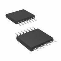
AT89LP214-20XU Atmel, AT89LP214-20XU Datasheet - Page 27

AT89LP214-20XU
Manufacturer Part Number
AT89LP214-20XU
Description
MCU 8051 2K FLASH 20MHZ 14-TSSOP
Manufacturer
Atmel
Series
89LPr
Datasheet
1.AT89LP213-20PU.pdf
(98 pages)
Specifications of AT89LP214-20XU
Core Processor
8051
Core Size
8-Bit
Speed
20MHz
Connectivity
SPI, UART/USART
Peripherals
Brown-out Detect/Reset, POR, PWM, WDT
Number Of I /o
12
Program Memory Size
2KB (2K x 8)
Program Memory Type
FLASH
Ram Size
128 x 8
Voltage - Supply (vcc/vdd)
2.4 V ~ 5.5 V
Oscillator Type
Internal
Operating Temperature
-40°C ~ 85°C
Package / Case
14-TSSOP
Package
14TSSOP
Device Core
8051
Family Name
AT89
Maximum Speed
20 MHz
Operating Supply Voltage
2.5|3.3|5 V
Data Bus Width
8 Bit
Number Of Programmable I/os
12
Interface Type
SPI/UART
Number Of Timers
2
Core
8051
Processor Series
AT89x
Maximum Clock Frequency
20 MHz
Data Ram Size
128 B
Mounting Style
SMD/SMT
Height
1.05 mm
Length
5.1 mm
Maximum Operating Temperature
+ 85 C
Minimum Operating Temperature
- 40 C
Supply Voltage (max)
5.5 V
Supply Voltage (min)
2.4 V
Width
4.5 mm
Lead Free Status / RoHS Status
Lead free / RoHS Compliant
Eeprom Size
-
Data Converters
-
Lead Free Status / Rohs Status
Details
13.3
13.4
13.5
3538E–MICRO–11/10
Port Read-modify-write
Ports During Powerdown
Port Alternate Functions
A read from a port will read either the state of the pins or the state of the port register depending
on which instruction is used. Simple read instructions will always access the port pins directly.
Read-modify-write instructions, which read a value, possibly modify it, and then write it back, will
always access the port register. This includes bit write instructions such as CLR or SETB as they
actually read the entire port, modify a single bit, then write the data back to the entire port. See
Table 13-3
Table 13-3.
Due to the 5V tolerant port structure, the output ports may have reduced V
under DC conditions, i.e. in the powerdown state, and at high temperature. It is recommended
that output ports be placed in a low state, if possible, prior to entering powerdown, or else exter-
nal pullups can be used to maintain the output at a higher voltage.
Most general-purpose digital I/O pins of the AT89LP213/214 share functionality with the various
I/Os needed for the peripheral units.
Alternate functions are connected to the pins in a logic AND fashion. In order to enable the
alternate function on a port pin, that pin must have a “1” in its corresponding port register bit,
otherwise the input/output will always be “0”. Furthermore, each pin must be configured
for the correct input/output mode as required by its peripheral before it may be used as such.
Table 13-4
Table 13-4.
Mnemonic
ANL
ORL
XRL
JBC
CPL
INC
DEC
DJNZ
MOV PX.Y, C
CLR PX.Y
SETB PX.Y
PxM0.y
0
0
1
1
for a complete list of Read-modify-write instruction which may access the ports.
shows how to configure a generic pin for use with an alternate function.
Port Read-modify-write Instructions
Alternate Function Configurations for Pin y of Port x
Instruction
Logical AND
Logical OR
Logical EX-OR
Jump if bit set and clear bit
Complement bit
Increment
Decrement
Decrement and jump if not zero
Move carry to bit Y of Port X
Clear bit Y of Port X
Set bit Y of Port X
PxM1.y
0
1
0
1
Table 13-5
Px.y
X
lists the alternate functions of the port pins.
1
1
1
bidirectional (internal pull-up)
output
input
bidirectional (external pull-up)
I/O Mode
AT89LP213/214
Example
ANL P1, A
ORL P1, A
XRL P1, A
JBC P3.0, LABEL
CPL P3.1
INC P1
DEC P3
DJNZ P3, LABEL
MOV P1.0, C
CLR P1.1
SETB P3.2
OH
while the device is
27


