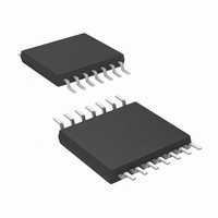
AT89LP214-20XU Atmel, AT89LP214-20XU Datasheet - Page 4

AT89LP214-20XU
Manufacturer Part Number
AT89LP214-20XU
Description
MCU 8051 2K FLASH 20MHZ 14-TSSOP
Manufacturer
Atmel
Series
89LPr
Datasheet
1.AT89LP213-20PU.pdf
(98 pages)
Specifications of AT89LP214-20XU
Core Processor
8051
Core Size
8-Bit
Speed
20MHz
Connectivity
SPI, UART/USART
Peripherals
Brown-out Detect/Reset, POR, PWM, WDT
Number Of I /o
12
Program Memory Size
2KB (2K x 8)
Program Memory Type
FLASH
Ram Size
128 x 8
Voltage - Supply (vcc/vdd)
2.4 V ~ 5.5 V
Oscillator Type
Internal
Operating Temperature
-40°C ~ 85°C
Package / Case
14-TSSOP
Package
14TSSOP
Device Core
8051
Family Name
AT89
Maximum Speed
20 MHz
Operating Supply Voltage
2.5|3.3|5 V
Data Bus Width
8 Bit
Number Of Programmable I/os
12
Interface Type
SPI/UART
Number Of Timers
2
Core
8051
Processor Series
AT89x
Maximum Clock Frequency
20 MHz
Data Ram Size
128 B
Mounting Style
SMD/SMT
Height
1.05 mm
Length
5.1 mm
Maximum Operating Temperature
+ 85 C
Minimum Operating Temperature
- 40 C
Supply Voltage (max)
5.5 V
Supply Voltage (min)
2.4 V
Width
4.5 mm
Lead Free Status / RoHS Status
Lead free / RoHS Compliant
Eeprom Size
-
Data Converters
-
Lead Free Status / Rohs Status
Details
Table 3-2.
4
Pin
10
11
12
13
14
1
2
3
4
5
6
7
8
9
Symbol
AT89LP213/214
GND
VCC
P1.5
P1.7
P1.3
P1.2
P3.0
P3.2
P3.3
P3.1
P1.0
P1.1
P1.4
P1.6
AT89LP214 Pin Description
Type
I/O
I/O
I/O
I/O
I/O
I/O
I/O
I/O
I/O
I/O
I/O
I/O
I/O
I/O
I/O
I/O
I/O
O
O
O
I
I
I
I
I
I
I
I
I
I
I
I
I
I
I
I
I
Description
P1.5: User-configurable I/O Port 1 bit 5.
MOSI: SPI master-out/slave-in. When configured as master, this pin is an output. When configured as
slave, this pin is an input.
GPI5: General-purpose Interrupt input 5.
P1.7: User-configurable I/O Port 1 bit 7.
SCK: SPI Clock. When configured as master, this pin is an output. When configured as slave, this pin is
an input.
GPI7: General-purpose Interrupt input 7.
P1.3: User-configurable I/O Port 1 bit 3 (if Reset Fuse is disabled).
RST: External Active-Low Reset input (if Reset Fuse is enabled.
GPI3: General-purpose Interrupt input 3.
DCL: Serial Clock input for On-chip Debug Interface.
Ground
P1.2: User-configurable I/O Port 1 bit 2.
GPI2: General-purpose Interrupt input 2.
P3.0: User-configurable I/O Port 3 bit 0.
RXD: Serial Port Receiver input.
P3.2: User-configurable I/O Port 3 bit 2.
XTAL1: Input to the inverting oscillator amplifier and internal clock generation circuits. It may be used as
a port pin if the internal RC oscillator is selected as the clock source.
DDA: Serial Data input/output for On-chip Debug Interface when OCD is enabled and the internal RC
oscillator is selected as the clock source.
P3.3: User-configurable I/O Port 3 bit 3.
XTAL2: Output from inverting oscillator amplifier. It may be used as a port pin if the internal
RC oscillator is selected as the clock source.
CLKOUT: When the internal RC oscillator is selected as the clock source, may be used to output the
internal clock divided by 2.
DDA: Serial Data input/output for On-chip Debug Interface when OCD is enabled and the external clock
is selected as the clock source.\
P3.1: User-configurable I/O Port 3 bit 1.
TXD: Serial Port Transmitter output.
Supply Voltage
P1.0: User-configurable I/O Port 1 bit 0.
AIN0: Analog Comparator Positive input.
GPI0: General-purpose Interrupt input 0.
P1.1: User-configurable I/O Port 1 bit 1.
AIN1: Analog Comparator Negative input.
GPI1: General-purpose Interrupt input 1
P1.4: User-configurable I/O Port 1 bit 4.
SS: SPI slave select input.
GPI4: General-purpose Interrupt input 4.
P1.6: User-configurable I/O Port 1 bit 6.
MISO: SPI master-in/slave-out. When configured as master, this pin is an input. When configured
as slave, this pin is an output.
GPI6: General-purpose Interrupt input 6.
See “External Reset” on page
3538E–MICRO–11/10
16).


