AT91SAM9R64-CU-999 Atmel, AT91SAM9R64-CU-999 Datasheet - Page 203
AT91SAM9R64-CU-999
Manufacturer Part Number
AT91SAM9R64-CU-999
Description
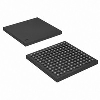
IC MCU ARM9 64K SRAM 144LFBGA
Manufacturer
Atmel
Series
AT91SAMr
Datasheet
1.AT91SAM9R64-CU.pdf
(903 pages)
Specifications of AT91SAM9R64-CU-999
Core Processor
ARM9
Core Size
16/32-Bit
Speed
240MHz
Connectivity
EBI/EMI, I²C, MMC, SPI, SSC, UART/USART, USB
Peripherals
AC'97, POR, PWM, WDT
Number Of I /o
49
Program Memory Size
32KB (32K x 8)
Program Memory Type
ROM
Ram Size
72K x 8
Voltage - Supply (vcc/vdd)
1.08 V ~ 1.32 V
Data Converters
A/D 3x10b
Oscillator Type
Internal
Operating Temperature
-40°C ~ 85°C
Package / Case
144-LFBGA
Processor Series
AT91SAMx
Core
ARM926EJ-S
Data Bus Width
32 bit
Data Ram Size
64 KB
Interface Type
SPI, TWI, UART
Maximum Clock Frequency
240 MHz
Number Of Programmable I/os
118
Operating Supply Voltage
1.65 V to 3.6 V
Maximum Operating Temperature
+ 85 C
Mounting Style
SMD/SMT
3rd Party Development Tools
JTRACE-ARM-2M, MDK-ARM, RL-ARM, ULINK2
Development Tools By Supplier
AT91SAM-ICE, AT91-ISP, AT91SAM9RL-EK
Minimum Operating Temperature
- 40 C
For Use With
AT91SAM-ICE - EMULATOR FOR AT91 ARM7/ARM9
Lead Free Status / RoHS Status
Lead free / RoHS Compliant
Eeprom Size
-
Lead Free Status / Rohs Status
Details
Available stocks
Company
Part Number
Manufacturer
Quantity
Price


22.14.4
Register Name:
Access Type:
• READ_MODE:
1: The read operation is controlled by the NRD signal.
0: The read operation is controlled by the NCS signal.
• WRITE_MODE
1: The write operation is controlled by the NWE signal.
0: The write operation is controlled by the NCS signal.
• EXNW_MODE: NWAIT Mode
The NWAIT signal is used to extend the current read or write signal. It is only taken into account during the pulse phase of
the read and write controlling signal. When the use of NWAIT is enabled, at least one cycle hold duration must be pro-
grammed for the read and write controlling signal.
6289C–ATARM–28-May-09
• Disabled Mode: The NWAIT input signal is ignored on the corresponding Chip Select.
• Frozen Mode: If asserted, the NWAIT signal freezes the current read or write cycle. After deassertion, the read/write
• Ready Mode: The NWAIT signal indicates the availability of the external device at the end of the pulse of the controlling
cycle is resumed from the point where it was stopped.
read or write signal, to complete the access. If high, the access normally completes. If low, the access is extended until
NWAIT returns high.
– If TDF cycles are programmed, the external bus is marked busy after the rising edge of NRD.
– If TDF optimization is enabled (TDF_MODE =1), TDF wait states are inserted after the setup of NRD.
– If TDF cycles are programmed, the external bus is marked busy after the rising edge of NCS.
– If TDF optimization is enabled (TDF_MODE =1), TDF wait states are inserted after the setup of NCS.
– If TDF optimization is enabled (TDF_MODE =1), TDF wait states will be inserted after the setup of NWE.
– If TDF optimization is enabled (TDF_MODE =1), TDF wait states will be inserted after the setup of NCS.
31
23
15
–
–
–
7
–
SMC MODE Register
0
0
1
1
EXNW_MODE
30
22
14
SMC_MODE[0..5]
Read/Write
–
–
–
6
–
0
1
0
1
29
21
13
–
5
EXNW_MODE
DBW
PS
TDF_MODE
NWAIT Mode
Disabled
Reserved
Frozen Mode
Ready Mode
28
20
12
4
AT91SAM9R64/RL64 Preliminary
27
19
11
–
–
3
–
26
18
10
–
–
2
–
TDF_CYCLES
WRITE_MODE
25
17
–
9
–
1
READ_MODE
PMEN
BAT
24
16
8
0
203
Related parts for AT91SAM9R64-CU-999
Image
Part Number
Description
Manufacturer
Datasheet
Request
R

Part Number:
Description:
MCU ARM9 64K SRAM 144-LFBGA
Manufacturer:
Atmel
Datasheet:

Part Number:
Description:
MCU, MPU & DSP Development Tools KICKSTART KIT FOR AT91SAM9 PLUS
Manufacturer:
IAR Systems

Part Number:
Description:
DEV KIT FOR AVR/AVR32
Manufacturer:
Atmel
Datasheet:

Part Number:
Description:
INTERVAL AND WIPE/WASH WIPER CONTROL IC WITH DELAY
Manufacturer:
ATMEL Corporation
Datasheet:
Part Number:
Description:
Low-Voltage Voice-Switched IC for Hands-Free Operation
Manufacturer:
ATMEL Corporation
Datasheet:
Part Number:
Description:
MONOLITHIC INTEGRATED FEATUREPHONE CIRCUIT
Manufacturer:
ATMEL Corporation
Datasheet:
Part Number:
Description:
AM-FM Receiver IC U4255BM-M
Manufacturer:
ATMEL Corporation
Datasheet:
Part Number:
Description:
Monolithic Integrated Feature Phone Circuit
Manufacturer:
ATMEL Corporation
Datasheet:
Part Number:
Description:
Multistandard Video-IF and Quasi Parallel Sound Processing
Manufacturer:
ATMEL Corporation
Datasheet:
Part Number:
Description:
High-performance EE PLD
Manufacturer:
ATMEL Corporation
Datasheet:
Part Number:
Description:
8-bit Flash Microcontroller
Manufacturer:
ATMEL Corporation
Datasheet: