AT91SAM9R64-CU-999 Atmel, AT91SAM9R64-CU-999 Datasheet - Page 82
AT91SAM9R64-CU-999
Manufacturer Part Number
AT91SAM9R64-CU-999
Description
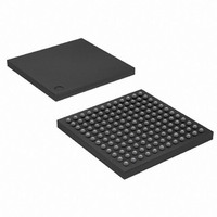
IC MCU ARM9 64K SRAM 144LFBGA
Manufacturer
Atmel
Series
AT91SAMr
Datasheet
1.AT91SAM9R64-CU.pdf
(903 pages)
Specifications of AT91SAM9R64-CU-999
Core Processor
ARM9
Core Size
16/32-Bit
Speed
240MHz
Connectivity
EBI/EMI, I²C, MMC, SPI, SSC, UART/USART, USB
Peripherals
AC'97, POR, PWM, WDT
Number Of I /o
49
Program Memory Size
32KB (32K x 8)
Program Memory Type
ROM
Ram Size
72K x 8
Voltage - Supply (vcc/vdd)
1.08 V ~ 1.32 V
Data Converters
A/D 3x10b
Oscillator Type
Internal
Operating Temperature
-40°C ~ 85°C
Package / Case
144-LFBGA
Processor Series
AT91SAMx
Core
ARM926EJ-S
Data Bus Width
32 bit
Data Ram Size
64 KB
Interface Type
SPI, TWI, UART
Maximum Clock Frequency
240 MHz
Number Of Programmable I/os
118
Operating Supply Voltage
1.65 V to 3.6 V
Maximum Operating Temperature
+ 85 C
Mounting Style
SMD/SMT
3rd Party Development Tools
JTRACE-ARM-2M, MDK-ARM, RL-ARM, ULINK2
Development Tools By Supplier
AT91SAM-ICE, AT91-ISP, AT91SAM9RL-EK
Minimum Operating Temperature
- 40 C
For Use With
AT91SAM-ICE - EMULATOR FOR AT91 ARM7/ARM9
Lead Free Status / RoHS Status
Lead free / RoHS Compliant
Eeprom Size
-
Lead Free Status / Rohs Status
Details
Available stocks
Company
Part Number
Manufacturer
Quantity
Price


14.7.3.2
14.8
6289C–ATARM–28-May-09
Hardware and Software Constraints
Communication Endpoints
The device also handles some class requests defined in the CDC class.
Table 14-4.
Unhandled requests are STALLed.
There are two communication endpoints and endpoint 0 is used for the enumeration process.
Endpoint 1 is a 512-byte Bulk OUT endpoint and endpoint 2 is a 512-byte Bulk IN endpoint.
SAM-BA Boot commands are sent by the host through the endpoint 1. If required, the message
is split by the host into several data payloads by the host driver.
If the command requires a response, the host can send IN transactions to pick up the response.
The MCI, the SPI and NAND Flash drivers use several PIOs in alternate functions to communi-
cate with devices. Care must be taken when these PIOs are used by the application. The
devices connected could be unintentionally driven at boot time, and electrical conflicts between
peripherals output pins and the connected devices may appear.
To assure correct functionality, it is recommended to plug in critical devices to other pins.
Table 14-5
are driven during the boot sequence for a period of less than 1 second if no correct boot program
is found.
For the DataFlash driven by the SPCK signal at 8 MHz, the time to download 60 K bytes is
reduced to 200 ms.
Request
SET_LINE_CODING
GET_LINE_CODING
SET_CONTROL_LINE_STATE
• A 12 MHz Crystal is mandatory in order to generate correctly 480 MHz clock necessary for
• No Bypass Mode.
• The SD Card, NAND Flash and DataFlash downloaded code size must be inferior to 56 K
• The code is always downloaded from the DataFlash or NAND Flash device address
• The downloaded code must be position-independent or linked at address 0x0000_0000.
• The DataFlash must be connected to NPCS0 of the SPI.
the USB High Speed Device and to generate the 48 MHz System clock.
bytes.
0x0000_0000 to the address 0x0000_0000 of the internal SRAM (after remap).
contains a list of pins that are driven during the boot program execution. These pins
Handled Class Requests
AT91SAM9R64/RL64 Preliminary
Definition
Configures DTE rate, stop bits, parity and number of
character bits.
Requests current DTE rate, stop bits, parity and number
of character bits.
RS-232 signal used to tell the DCE device the DTE
device is now present.
82
Related parts for AT91SAM9R64-CU-999
Image
Part Number
Description
Manufacturer
Datasheet
Request
R

Part Number:
Description:
MCU ARM9 64K SRAM 144-LFBGA
Manufacturer:
Atmel
Datasheet:

Part Number:
Description:
MCU, MPU & DSP Development Tools KICKSTART KIT FOR AT91SAM9 PLUS
Manufacturer:
IAR Systems

Part Number:
Description:
DEV KIT FOR AVR/AVR32
Manufacturer:
Atmel
Datasheet:

Part Number:
Description:
INTERVAL AND WIPE/WASH WIPER CONTROL IC WITH DELAY
Manufacturer:
ATMEL Corporation
Datasheet:
Part Number:
Description:
Low-Voltage Voice-Switched IC for Hands-Free Operation
Manufacturer:
ATMEL Corporation
Datasheet:
Part Number:
Description:
MONOLITHIC INTEGRATED FEATUREPHONE CIRCUIT
Manufacturer:
ATMEL Corporation
Datasheet:
Part Number:
Description:
AM-FM Receiver IC U4255BM-M
Manufacturer:
ATMEL Corporation
Datasheet:
Part Number:
Description:
Monolithic Integrated Feature Phone Circuit
Manufacturer:
ATMEL Corporation
Datasheet:
Part Number:
Description:
Multistandard Video-IF and Quasi Parallel Sound Processing
Manufacturer:
ATMEL Corporation
Datasheet:
Part Number:
Description:
High-performance EE PLD
Manufacturer:
ATMEL Corporation
Datasheet:
Part Number:
Description:
8-bit Flash Microcontroller
Manufacturer:
ATMEL Corporation
Datasheet: