AT91SAM9R64-CU-999 Atmel, AT91SAM9R64-CU-999 Datasheet - Page 712
AT91SAM9R64-CU-999
Manufacturer Part Number
AT91SAM9R64-CU-999
Description
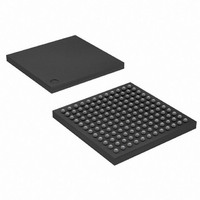
IC MCU ARM9 64K SRAM 144LFBGA
Manufacturer
Atmel
Series
AT91SAMr
Datasheet
1.AT91SAM9R64-CU.pdf
(903 pages)
Specifications of AT91SAM9R64-CU-999
Core Processor
ARM9
Core Size
16/32-Bit
Speed
240MHz
Connectivity
EBI/EMI, I²C, MMC, SPI, SSC, UART/USART, USB
Peripherals
AC'97, POR, PWM, WDT
Number Of I /o
49
Program Memory Size
32KB (32K x 8)
Program Memory Type
ROM
Ram Size
72K x 8
Voltage - Supply (vcc/vdd)
1.08 V ~ 1.32 V
Data Converters
A/D 3x10b
Oscillator Type
Internal
Operating Temperature
-40°C ~ 85°C
Package / Case
144-LFBGA
Processor Series
AT91SAMx
Core
ARM926EJ-S
Data Bus Width
32 bit
Data Ram Size
64 KB
Interface Type
SPI, TWI, UART
Maximum Clock Frequency
240 MHz
Number Of Programmable I/os
118
Operating Supply Voltage
1.65 V to 3.6 V
Maximum Operating Temperature
+ 85 C
Mounting Style
SMD/SMT
3rd Party Development Tools
JTRACE-ARM-2M, MDK-ARM, RL-ARM, ULINK2
Development Tools By Supplier
AT91SAM-ICE, AT91-ISP, AT91SAM9RL-EK
Minimum Operating Temperature
- 40 C
For Use With
AT91SAM-ICE - EMULATOR FOR AT91 ARM7/ARM9
Lead Free Status / RoHS Status
Lead free / RoHS Compliant
Eeprom Size
-
Lead Free Status / Rohs Status
Details
Available stocks
Company
Part Number
Manufacturer
Quantity
Price


40.6.2.1
40.6.2.2
712
AT91SAM9R64/RL64 Preliminary
AC97 Controller Setup
Transmit Operation
The following operations must be performed in order to bring the AC’97 Controller into an oper-
ating state:
The application must perform the following steps in order to send data via a channel to the AC97
Codec:
Once data has been transferred to the Channel x Shift Register, the TXRDY flag is automatically
set by the AC’97 Controller which allows the application to start a new write action. The applica-
tion can also wait for an interrupt notice associated with TXRDY in order to send data. The
interrupt remains active until TXRDY flag is cleared..
1. Enable the AC97 Controller clock in the PMC controller.
2. Turn on AC97 function by enabling the ENA bit in AC97 Controller Mode Register
3. Configure the input channel assignment by controlling the AC’97 Controller Input
4. Configure the output channel assignment by controlling the AC’97 Controller Input
5. Configure sample width for Channel A and Channel B by writing the SIZE bit field in
6. Configure data Endianness for Channel A and Channel B by writing CEM bit field in
7. Configure the PIO controller to drive the RESET signal of the external Codec. The
8. Enable Channel A and/or Channel B by writing CEN bit field in AC97C_CAMR and
• Check if previous data has been sent by polling TXRDY flag in the AC97C Channel x Status
• Write data to the AC’97 Controller Channel x Transmit Holding Register (AC97C_CxTHR).
Register (AC97_CxSR). x being one of the
(AC97C_MR).
Assignment Register (AC97C_ICA).
Assignment Register (AC97C_OCA).
AC97C Channel A Mode Register (AC97C_CAMR) and AC97C Channel B Mode Reg-
ister (AC97C_CBMR). The application can write 10, 16, 18,or 20-bit wide PCM samples
through the AC’97 interface and they will be transferred into 20-bit wide slots.
AC97C_CAMR and AC97C_CBMR registers. Data on the AC-link are shifted MSB first.
The application can write little- or big-endian data to the AC’97 Controller interface.
RESET signal must fulfill external AC97 Codec timing requirements.
AC97C_CBMR registers.
2
channels.
6289C–ATARM–28-May-09
Related parts for AT91SAM9R64-CU-999
Image
Part Number
Description
Manufacturer
Datasheet
Request
R

Part Number:
Description:
MCU ARM9 64K SRAM 144-LFBGA
Manufacturer:
Atmel
Datasheet:

Part Number:
Description:
MCU, MPU & DSP Development Tools KICKSTART KIT FOR AT91SAM9 PLUS
Manufacturer:
IAR Systems

Part Number:
Description:
DEV KIT FOR AVR/AVR32
Manufacturer:
Atmel
Datasheet:

Part Number:
Description:
INTERVAL AND WIPE/WASH WIPER CONTROL IC WITH DELAY
Manufacturer:
ATMEL Corporation
Datasheet:
Part Number:
Description:
Low-Voltage Voice-Switched IC for Hands-Free Operation
Manufacturer:
ATMEL Corporation
Datasheet:
Part Number:
Description:
MONOLITHIC INTEGRATED FEATUREPHONE CIRCUIT
Manufacturer:
ATMEL Corporation
Datasheet:
Part Number:
Description:
AM-FM Receiver IC U4255BM-M
Manufacturer:
ATMEL Corporation
Datasheet:
Part Number:
Description:
Monolithic Integrated Feature Phone Circuit
Manufacturer:
ATMEL Corporation
Datasheet:
Part Number:
Description:
Multistandard Video-IF and Quasi Parallel Sound Processing
Manufacturer:
ATMEL Corporation
Datasheet:
Part Number:
Description:
High-performance EE PLD
Manufacturer:
ATMEL Corporation
Datasheet:
Part Number:
Description:
8-bit Flash Microcontroller
Manufacturer:
ATMEL Corporation
Datasheet: