AT91SAM9R64-CU-999 Atmel, AT91SAM9R64-CU-999 Datasheet - Page 25
AT91SAM9R64-CU-999
Manufacturer Part Number
AT91SAM9R64-CU-999
Description
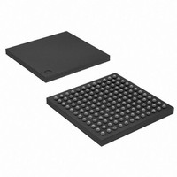
IC MCU ARM9 64K SRAM 144LFBGA
Manufacturer
Atmel
Series
AT91SAMr
Datasheet
1.AT91SAM9R64-CU.pdf
(903 pages)
Specifications of AT91SAM9R64-CU-999
Core Processor
ARM9
Core Size
16/32-Bit
Speed
240MHz
Connectivity
EBI/EMI, I²C, MMC, SPI, SSC, UART/USART, USB
Peripherals
AC'97, POR, PWM, WDT
Number Of I /o
49
Program Memory Size
32KB (32K x 8)
Program Memory Type
ROM
Ram Size
72K x 8
Voltage - Supply (vcc/vdd)
1.08 V ~ 1.32 V
Data Converters
A/D 3x10b
Oscillator Type
Internal
Operating Temperature
-40°C ~ 85°C
Package / Case
144-LFBGA
Processor Series
AT91SAMx
Core
ARM926EJ-S
Data Bus Width
32 bit
Data Ram Size
64 KB
Interface Type
SPI, TWI, UART
Maximum Clock Frequency
240 MHz
Number Of Programmable I/os
118
Operating Supply Voltage
1.65 V to 3.6 V
Maximum Operating Temperature
+ 85 C
Mounting Style
SMD/SMT
3rd Party Development Tools
JTRACE-ARM-2M, MDK-ARM, RL-ARM, ULINK2
Development Tools By Supplier
AT91SAM-ICE, AT91-ISP, AT91SAM9RL-EK
Minimum Operating Temperature
- 40 C
For Use With
AT91SAM-ICE - EMULATOR FOR AT91 ARM7/ARM9
Lead Free Status / RoHS Status
Lead free / RoHS Compliant
Eeprom Size
-
Lead Free Status / Rohs Status
Details
Available stocks
Company
Part Number
Manufacturer
Quantity
Price


8.1.1.2
8.1.2
8.1.2.1
8.1.2.2
6289C–ATARM–28-May-09
Boot Strategies
Internal ROM
BMS = 1, boot on embedded ROM
BMS = 0, boot on external memory
When accessed from the AHB, the internal Fast SRAM is single cycle accessible at full matrix
speed (MCK). When accessed from the processor’s TCM Interface, they are also single cycle
accessible at full processor speed.
The AT91SAM9R64/RL64 embeds an Internal ROM, which contains the SAM-BA program.
At any time, the ROM is mapped at address 0x0040 0000. It is also accessible at address 0x0
(BMS =1) after the reset and before the Remap Command.
The system always boots at address 0x0. To ensure maximum boot possibilities, the memory
layout can be changed with two parameters.
REMAP allows the user to layout the internal SRAM bank to 0x0 to ease the development. This
is done by software once the system has boot. Refer to the Bus Matrix Section for more details.
When REMAP = 0 BMS allows the user to lay out to 0x0, at his convenience, the ROM or an
external memory. This is done by a hardware way at reset.
Note: All the memory blocks can always be seen at their specified base addresses that are not
concerned by these parameters.
The AT91SAM9R64/RL64 Bus Matrix manages a boot memory that depends on the level on the
pin BMS at reset. The internal memory area mapped between address 0x0 and 0x000F FFFF is
reserved to this effect.
If BMS is detected at 1, the boot memory is the embedded ROM.
If BMS is detected at 0, the boot memory is the memory connected on the Chip Select 0 of the
External Bus Interface.
The system boots on Boot Program.
• Boot on on-chip RC
• Enable the 32768 Hz oscillator
• Auto baudrate detection
• Downloads and runs an application from external storage media into internal SRAM
• Downloaded code size depends on embedded SRAM size
• Automatic detection of valid application
• Bootloader on a non-volatile memory
• SAM-BA Boot in case no valid program is detected in external NVM, supporting
• Boot on on-chip RC
– SDCard (boot ROM does not support high-capacity SDCards)
– NAND Flash
– SPI DataFlash
– Serial communication on a DBGU
– USB Device HS Port
®
connected on NPCS0 of the SPI0
AT91SAM9R64/RL64 Preliminary
25
Related parts for AT91SAM9R64-CU-999
Image
Part Number
Description
Manufacturer
Datasheet
Request
R

Part Number:
Description:
MCU ARM9 64K SRAM 144-LFBGA
Manufacturer:
Atmel
Datasheet:

Part Number:
Description:
MCU, MPU & DSP Development Tools KICKSTART KIT FOR AT91SAM9 PLUS
Manufacturer:
IAR Systems

Part Number:
Description:
DEV KIT FOR AVR/AVR32
Manufacturer:
Atmel
Datasheet:

Part Number:
Description:
INTERVAL AND WIPE/WASH WIPER CONTROL IC WITH DELAY
Manufacturer:
ATMEL Corporation
Datasheet:
Part Number:
Description:
Low-Voltage Voice-Switched IC for Hands-Free Operation
Manufacturer:
ATMEL Corporation
Datasheet:
Part Number:
Description:
MONOLITHIC INTEGRATED FEATUREPHONE CIRCUIT
Manufacturer:
ATMEL Corporation
Datasheet:
Part Number:
Description:
AM-FM Receiver IC U4255BM-M
Manufacturer:
ATMEL Corporation
Datasheet:
Part Number:
Description:
Monolithic Integrated Feature Phone Circuit
Manufacturer:
ATMEL Corporation
Datasheet:
Part Number:
Description:
Multistandard Video-IF and Quasi Parallel Sound Processing
Manufacturer:
ATMEL Corporation
Datasheet:
Part Number:
Description:
High-performance EE PLD
Manufacturer:
ATMEL Corporation
Datasheet:
Part Number:
Description:
8-bit Flash Microcontroller
Manufacturer:
ATMEL Corporation
Datasheet: