AT91SAM9R64-CU-999 Atmel, AT91SAM9R64-CU-999 Datasheet - Page 633
AT91SAM9R64-CU-999
Manufacturer Part Number
AT91SAM9R64-CU-999
Description
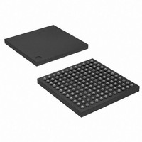
IC MCU ARM9 64K SRAM 144LFBGA
Manufacturer
Atmel
Series
AT91SAMr
Datasheet
1.AT91SAM9R64-CU.pdf
(903 pages)
Specifications of AT91SAM9R64-CU-999
Core Processor
ARM9
Core Size
16/32-Bit
Speed
240MHz
Connectivity
EBI/EMI, I²C, MMC, SPI, SSC, UART/USART, USB
Peripherals
AC'97, POR, PWM, WDT
Number Of I /o
49
Program Memory Size
32KB (32K x 8)
Program Memory Type
ROM
Ram Size
72K x 8
Voltage - Supply (vcc/vdd)
1.08 V ~ 1.32 V
Data Converters
A/D 3x10b
Oscillator Type
Internal
Operating Temperature
-40°C ~ 85°C
Package / Case
144-LFBGA
Processor Series
AT91SAMx
Core
ARM926EJ-S
Data Bus Width
32 bit
Data Ram Size
64 KB
Interface Type
SPI, TWI, UART
Maximum Clock Frequency
240 MHz
Number Of Programmable I/os
118
Operating Supply Voltage
1.65 V to 3.6 V
Maximum Operating Temperature
+ 85 C
Mounting Style
SMD/SMT
3rd Party Development Tools
JTRACE-ARM-2M, MDK-ARM, RL-ARM, ULINK2
Development Tools By Supplier
AT91SAM-ICE, AT91-ISP, AT91SAM9RL-EK
Minimum Operating Temperature
- 40 C
For Use With
AT91SAM-ICE - EMULATOR FOR AT91 ARM7/ARM9
Lead Free Status / RoHS Status
Lead free / RoHS Compliant
Eeprom Size
-
Lead Free Status / Rohs Status
Details
Available stocks
Company
Part Number
Manufacturer
Quantity
Price


38.9.2
Name:
Access Type:
• CLKDIV: Clock Divider
Multimedia Card Interface clock (MCCK or MCI_CK) is Master Clock (MCK) divided by (2*(CLKDIV+1)).
• PWSDIV: Power Saving Divider
Multimedia Card Interface clock is divided by 2
Warning: This value must be different from 0 before enabling the Power Save Mode in the MCI_CR (MCI_PWSEN bit).
• RDPROOF Read Proof Enable
Enabling Read Proof allows to stop the MCI Clock during read access if the internal FIFO is full. This guarantees data
integrity, not bandwidth.
0 = Disables Read Proof.
1 = Enables Read Proof.
• WRPROOF Write Proof Enable
Enabling Write Proof allows to stop the MCI Clock during write access if the internal FIFO is full. This guarantees data
integrity, not bandwidth.
0 = Disables Write Proof.
1 = Enables Write Proof.
• PDCFBYTE: PDC Force Byte Transfer
Enabling PDC Force Byte Transfer allows the PDC to manage with internal byte transfers, so that transfer of blocks with a
size different from modulo 4 can be supported.
Warning: BLKLEN value depends on PDCFBYTE.
0 = Disables PDC Force Byte Transfer. PDC type of transfer are in words.
1 = Enables PDC Force Byte Transfer. PDC type of transfer are in bytes.
• PDCPADV: PDC Padding Value
0 = 0x00 value is used when padding data in write transfer (not only PDC transfer).
1 = 0xFF value is used when padding data in write transfer (not only PDC transfer).
6289C–ATARM–28-May-09
PDCMODE
31
23
15
7
MCI Mode Register
PDCPADV
30
22
14
MCI_MR
Read/write
6
PDCFBYTE
29
21
13
5
(PWSDIV)
WRPROOF
28
20
12
4
+ 1 when entering Power Saving Mode.
BLKLEN
BLKLEN
CLKDIV
AT91SAM9R64/RL64 Preliminary
RDPROOF
27
19
11
3
26
18
10
2
PWSDIV
25
17
9
1
24
16
8
0
633
Related parts for AT91SAM9R64-CU-999
Image
Part Number
Description
Manufacturer
Datasheet
Request
R

Part Number:
Description:
MCU ARM9 64K SRAM 144-LFBGA
Manufacturer:
Atmel
Datasheet:

Part Number:
Description:
MCU, MPU & DSP Development Tools KICKSTART KIT FOR AT91SAM9 PLUS
Manufacturer:
IAR Systems

Part Number:
Description:
DEV KIT FOR AVR/AVR32
Manufacturer:
Atmel
Datasheet:

Part Number:
Description:
INTERVAL AND WIPE/WASH WIPER CONTROL IC WITH DELAY
Manufacturer:
ATMEL Corporation
Datasheet:
Part Number:
Description:
Low-Voltage Voice-Switched IC for Hands-Free Operation
Manufacturer:
ATMEL Corporation
Datasheet:
Part Number:
Description:
MONOLITHIC INTEGRATED FEATUREPHONE CIRCUIT
Manufacturer:
ATMEL Corporation
Datasheet:
Part Number:
Description:
AM-FM Receiver IC U4255BM-M
Manufacturer:
ATMEL Corporation
Datasheet:
Part Number:
Description:
Monolithic Integrated Feature Phone Circuit
Manufacturer:
ATMEL Corporation
Datasheet:
Part Number:
Description:
Multistandard Video-IF and Quasi Parallel Sound Processing
Manufacturer:
ATMEL Corporation
Datasheet:
Part Number:
Description:
High-performance EE PLD
Manufacturer:
ATMEL Corporation
Datasheet:
Part Number:
Description:
8-bit Flash Microcontroller
Manufacturer:
ATMEL Corporation
Datasheet: