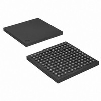
AT91SAM9R64-CU-999 Atmel, AT91SAM9R64-CU-999 Datasheet - Page 211

AT91SAM9R64-CU-999
Manufacturer Part Number
AT91SAM9R64-CU-999
Description
IC MCU ARM9 64K SRAM 144LFBGA
Manufacturer
Atmel
Series
AT91SAMr
Datasheet
1.AT91SAM9R64-CU.pdf
(903 pages)
Specifications of AT91SAM9R64-CU-999
Core Processor
ARM9
Core Size
16/32-Bit
Speed
240MHz
Connectivity
EBI/EMI, I²C, MMC, SPI, SSC, UART/USART, USB
Peripherals
AC'97, POR, PWM, WDT
Number Of I /o
49
Program Memory Size
32KB (32K x 8)
Program Memory Type
ROM
Ram Size
72K x 8
Voltage - Supply (vcc/vdd)
1.08 V ~ 1.32 V
Data Converters
A/D 3x10b
Oscillator Type
Internal
Operating Temperature
-40°C ~ 85°C
Package / Case
144-LFBGA
Processor Series
AT91SAMx
Core
ARM926EJ-S
Data Bus Width
32 bit
Data Ram Size
64 KB
Interface Type
SPI, TWI, UART
Maximum Clock Frequency
240 MHz
Number Of Programmable I/os
118
Operating Supply Voltage
1.65 V to 3.6 V
Maximum Operating Temperature
+ 85 C
Mounting Style
SMD/SMT
3rd Party Development Tools
JTRACE-ARM-2M, MDK-ARM, RL-ARM, ULINK2
Development Tools By Supplier
AT91SAM-ICE, AT91-ISP, AT91SAM9RL-EK
Minimum Operating Temperature
- 40 C
For Use With
AT91SAM-ICE - EMULATOR FOR AT91 ARM7/ARM9
Lead Free Status / RoHS Status
Lead free / RoHS Compliant
Eeprom Size
-
Lead Free Status / Rohs Status
Details
Available stocks
Company
Part Number
Manufacturer
Quantity
Price
- Current page: 211 of 903
- Download datasheet (13Mb)
23.5.2
Figure 23-3. Read Burst, 32-bit SDRAM Access
6289C–ATARM–28-May-09
SDRAM Controller Read Cycle
SDRAMC_A[12:0]
D[31:0]
SDWE
SDCS
(Input)
SDCK
RAS
CAS
The SDRAM Controller allows burst access, incremental burst of unspecified length or single
access. In all cases, the SDRAM Controller keeps track of the active row in each bank, thus
maximizing performance of the SDRAM. If row and bank addresses do not match the previous
row/bank address, then the SDRAM controller automatically generates a precharge command,
activates the new row and starts the read command. To comply with the SDRAM timing param-
eters, additional clock cycles on SDCK are inserted between precharge and active commands
(t
uration register of the SDRAM Controller. After a read command, additional wait states are
generated to comply with the CAS latency (1, 2 or 3 clock delays specified in the configuration
register).
For a single access or an incremented burst of unspecified length, the SDRAM Controller antici-
pates the next access. While the last value of the column is returned by the SDRAM Controller
on the bus, the SDRAM Controller anticipates the read to the next column and thus anticipates
the CAS latency. This reduces the effect of the CAS latency on the internal bus.
For burst access of specified length (4, 8, 16 words), access is not anticipated. This case leads
to the best performance. If the burst is broken (border, busy mode, etc.), the next access is han-
dled as an incrementing burst of unspecified length.
RP
) and between active and read command (t
Row n
t
RCD
= 3
col a
CAS = 2
AT91SAM9R64/RL64 Preliminary
col b
Dna
col c
Dnb
RCD
col d
). These two parameters are set in the config-
Dnc
col e
Dnd
col f
Dne
Dnf
211
Related parts for AT91SAM9R64-CU-999
Image
Part Number
Description
Manufacturer
Datasheet
Request
R

Part Number:
Description:
MCU ARM9 64K SRAM 144-LFBGA
Manufacturer:
Atmel
Datasheet:

Part Number:
Description:
MCU, MPU & DSP Development Tools KICKSTART KIT FOR AT91SAM9 PLUS
Manufacturer:
IAR Systems

Part Number:
Description:
DEV KIT FOR AVR/AVR32
Manufacturer:
Atmel
Datasheet:

Part Number:
Description:
INTERVAL AND WIPE/WASH WIPER CONTROL IC WITH DELAY
Manufacturer:
ATMEL Corporation
Datasheet:

Part Number:
Description:
Low-Voltage Voice-Switched IC for Hands-Free Operation
Manufacturer:
ATMEL Corporation
Datasheet:

Part Number:
Description:
MONOLITHIC INTEGRATED FEATUREPHONE CIRCUIT
Manufacturer:
ATMEL Corporation
Datasheet:

Part Number:
Description:
AM-FM Receiver IC U4255BM-M
Manufacturer:
ATMEL Corporation
Datasheet:

Part Number:
Description:
Monolithic Integrated Feature Phone Circuit
Manufacturer:
ATMEL Corporation
Datasheet:

Part Number:
Description:
Multistandard Video-IF and Quasi Parallel Sound Processing
Manufacturer:
ATMEL Corporation
Datasheet:

Part Number:
Description:
High-performance EE PLD
Manufacturer:
ATMEL Corporation
Datasheet:

Part Number:
Description:
8-bit Flash Microcontroller
Manufacturer:
ATMEL Corporation
Datasheet:


