MC908MR32CFUE Freescale Semiconductor, MC908MR32CFUE Datasheet - Page 146
MC908MR32CFUE
Manufacturer Part Number
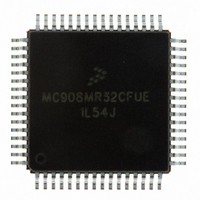
MC908MR32CFUE
Description
IC MCU 8MHZ 32K FLASH 64-QFP
Manufacturer
Freescale Semiconductor
Series
HC08r
Datasheet
1.MC908MR16CFUE.pdf
(282 pages)
Specifications of MC908MR32CFUE
Core Processor
HC08
Core Size
8-Bit
Speed
8MHz
Connectivity
SCI, SPI
Peripherals
LVD, POR, PWM
Number Of I /o
44
Program Memory Size
32KB (32K x 8)
Program Memory Type
FLASH
Ram Size
768 x 8
Voltage - Supply (vcc/vdd)
4.5 V ~ 5.5 V
Data Converters
A/D 10x10b
Oscillator Type
Internal
Operating Temperature
-40°C ~ 85°C
Package / Case
64-QFP
Processor Series
HC08MR
Core
HC08
Data Bus Width
8 bit
Data Ram Size
768 B
Interface Type
SCI/SPI
Maximum Clock Frequency
8.2 MHz
Number Of Programmable I/os
44
Number Of Timers
6
Operating Supply Voltage
0 V to 5 V
Maximum Operating Temperature
+ 85 C
Mounting Style
SMD/SMT
Development Tools By Supplier
FSICEBASE, M68CBL05CE
Minimum Operating Temperature
- 40 C
On-chip Adc
10-ch x 10-bit
Lead Free Status / RoHS Status
Lead free / RoHS Compliant
Eeprom Size
-
Lead Free Status / Rohs Status
Lead free / RoHS Compliant
Available stocks
Company
Part Number
Manufacturer
Quantity
Price

Company:
Part Number:
MC908MR32CFUE
Manufacturer:
Freescale Semiconductor
Quantity:
10 000
Part Number:
MC908MR32CFUE
Manufacturer:
NXP/恩智浦
Quantity:
20 000


Pulse-Width Modulator for Motor Control (PWMMC)
12.9.4 PWM Control Register 1
PWM control register 1 (PCTL1) controls PWM enabling/disabling, the loading of new modulus, prescaler,
PWM values, and the PWM correction method. In addition, this register contains the software disable bits
to force the PWM outputs to their inactive states (according to the disable mapping register).
DISX — Software Disable Bit for Bank X Bit
DISY — Software Disable Bit for Bank Y Bit
PWMINT — PWM Interrupt Enable Bit
PWMF — PWM Reload Flag
ISENS1 and ISENS0 — Current Sense Correction Bits
146
This read/write bit allows the user to disable one or more PWM pins in bank X. The pins that are
disabled are determined by the disable mapping write-once register.
This read/write bit allows the user to disable one or more PWM pins in bank Y. The pins that are
disabled are determined by the disable mapping write-once register.
This read/write bit allows the user to enable and disable PWM CPU interrupts. If set, a CPU interrupt
will be pending when the PWMF flag is set.
This read/write bit is set at the beginning of every reload cycle regardless of the state of the LDOK bit.
This bit is cleared by reading PWM control register 1 with the PWMF flag set, then writing a logic 0 to
PWMF. If another reload occurs before the clearing sequence is complete, then writing logic 0 to
PWMF has no effect.
These read/write bits select the top/bottom correction scheme as shown in
1 = Disable PWM pins in bank X.
0 = Re-enable PWM pins at beginning of next PWM cycle.
1 = Disable PWM pins in bank Y.
0 = Re-enable PWM pins at beginning of next PWM cycle.
1 = Enable PWM CPU interrupts.
0 = Disable PWM CPU interrupts.
1 = New reload cycle began.
0 = New reload cycle has not begun.
Address:
Reset:
When PWMINT is cleared, pending CPU interrupts are inhibited.
When PWMF is cleared, pending PWM CPU interrupts are cleared (not
including fault interrupts).
Read:
Write:
$0020
DISX
Bit 7
0
Figure 12-39. PWM Control Register 1 (PCTL1)
MC68HC908MR32 • MC68HC908MR16 Data Sheet, Rev. 6.1
DISY
6
0
PWMINT
5
0
PWMF
NOTE
NOTE
4
0
ISENS1
3
0
ISENS0
2
0
LDOK
1
0
Table
Freescale Semiconductor
PWMEN
12-7.
Bit 0
0
Related parts for MC908MR32CFUE
Image
Part Number
Description
Manufacturer
Datasheet
Request
R

Part Number:
Description:
Manufacturer:
Freescale Semiconductor, Inc
Datasheet:
Part Number:
Description:
Manufacturer:
Freescale Semiconductor, Inc
Datasheet:
Part Number:
Description:
Manufacturer:
Freescale Semiconductor, Inc
Datasheet:
Part Number:
Description:
Manufacturer:
Freescale Semiconductor, Inc
Datasheet:
Part Number:
Description:
Manufacturer:
Freescale Semiconductor, Inc
Datasheet:
Part Number:
Description:
Manufacturer:
Freescale Semiconductor, Inc
Datasheet:
Part Number:
Description:
Manufacturer:
Freescale Semiconductor, Inc
Datasheet:
Part Number:
Description:
Manufacturer:
Freescale Semiconductor, Inc
Datasheet:
Part Number:
Description:
Manufacturer:
Freescale Semiconductor, Inc
Datasheet:
Part Number:
Description:
Manufacturer:
Freescale Semiconductor, Inc
Datasheet:
Part Number:
Description:
Manufacturer:
Freescale Semiconductor, Inc
Datasheet:
Part Number:
Description:
Manufacturer:
Freescale Semiconductor, Inc
Datasheet:
Part Number:
Description:
Manufacturer:
Freescale Semiconductor, Inc
Datasheet:
Part Number:
Description:
Manufacturer:
Freescale Semiconductor, Inc
Datasheet:
Part Number:
Description:
Manufacturer:
Freescale Semiconductor, Inc
Datasheet: