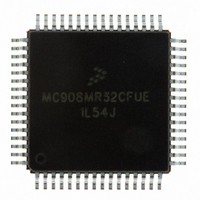
MC908MR32CFUE Freescale Semiconductor, MC908MR32CFUE Datasheet - Page 225

MC908MR32CFUE
Manufacturer Part Number
MC908MR32CFUE
Description
IC MCU 8MHZ 32K FLASH 64-QFP
Manufacturer
Freescale Semiconductor
Series
HC08r
Datasheet
1.MC908MR16CFUE.pdf
(282 pages)
Specifications of MC908MR32CFUE
Core Processor
HC08
Core Size
8-Bit
Speed
8MHz
Connectivity
SCI, SPI
Peripherals
LVD, POR, PWM
Number Of I /o
44
Program Memory Size
32KB (32K x 8)
Program Memory Type
FLASH
Ram Size
768 x 8
Voltage - Supply (vcc/vdd)
4.5 V ~ 5.5 V
Data Converters
A/D 10x10b
Oscillator Type
Internal
Operating Temperature
-40°C ~ 85°C
Package / Case
64-QFP
Processor Series
HC08MR
Core
HC08
Data Bus Width
8 bit
Data Ram Size
768 B
Interface Type
SCI/SPI
Maximum Clock Frequency
8.2 MHz
Number Of Programmable I/os
44
Number Of Timers
6
Operating Supply Voltage
0 V to 5 V
Maximum Operating Temperature
+ 85 C
Mounting Style
SMD/SMT
Development Tools By Supplier
FSICEBASE, M68CBL05CE
Minimum Operating Temperature
- 40 C
On-chip Adc
10-ch x 10-bit
Lead Free Status / RoHS Status
Lead free / RoHS Compliant
Eeprom Size
-
Lead Free Status / Rohs Status
Lead free / RoHS Compliant
Available stocks
Company
Part Number
Manufacturer
Quantity
Price
Company:
Part Number:
MC908MR32CFUE
Manufacturer:
Freescale Semiconductor
Quantity:
10 000
Part Number:
MC908MR32CFUE
Manufacturer:
NXP/恩智浦
Quantity:
20 000
- Current page: 225 of 282
- Download datasheet (2Mb)
The TIMA remains active after the execution of a WAIT instruction. In wait mode, the TIMA registers are
not accessible by the CPU. Any enabled CPU interrupt request from the TIMA can bring the MCU out of
wait mode.
If TIMA functions are not required during wait mode, reduce power consumption by stopping the TIMA
before executing the WAIT instruction.
16.6 I/O Signals
Port E shares five of its pins with the TIMA:
16.6.1 TIMA Clock Pin (PTE3/TCLKA)
PTE3/TCLKA is an external clock input that can be the clock source for the TIMA counter instead of the
prescaled internal bus clock. Select the PTE3/TCLKA input by writing logic 1s to the three prescaler select
bits, PS[2:0]. See
The maximum TCLK frequency is the least: 4 MHz or bus frequency ÷ 2.
PTE3/TCLKA is available as a general-purpose I/O pin when not used as the TIMA clock input. When the
PTE3/TCLKA pin is the TIMA clock input, it is an input regardless of the state of the DDRE3 bit in data
direction register E.
16.6.2 TIMA Channel I/O Pins (PTE4/TCH0A–PTE7/TCH3A)
Each channel I/O pin is programmable independently as an input capture pin or an output compare pin.
PTE2/TCH0 and PTE4/TCH2 can be configured as buffered output compare or buffered PWM pins.
16.7 I/O Registers
These input/output (I/O) registers control and monitor TIMA operation:
16.7.1 TIMA Status and Control Register
The TIMA status and control register:
Freescale Semiconductor
•
•
•
•
•
•
•
•
•
•
•
•
PTE3/TCLKA is an external clock input to the TIMA prescaler.
The four TIMA channel I/O pins are PTE4/TCH0A, PTE5/TCH1A, PTE6/TCH2A, and
PTE7/TCH3A.
TIMA status and control register (TASC)
TIMA control registers (TACNTH–TACNTL)
TIMA counter modulo registers (TAMODH–TAMODL)
TIMA channel status and control registers (TASC0, TASC1, TASC2, and TASC3)
TIMA channel registers (TACH0H–TACH0L, TACH1H–TACH1L, TACH2H–TACH2L, and
TACH3H–TACH3L)
Enables TIMA overflow interrupts
Flags TIMA overflows
Stops the TIMA counter
Resets the TIMA counter
Prescales the TIMA counter clock
16.7.1 TIMA Status and Control
MC68HC908MR32 • MC68HC908MR16 Data Sheet, Rev. 6.1
Register.
I/O Signals
225
Related parts for MC908MR32CFUE
Image
Part Number
Description
Manufacturer
Datasheet
Request
R
Part Number:
Description:
Manufacturer:
Freescale Semiconductor, Inc
Datasheet:
Part Number:
Description:
Manufacturer:
Freescale Semiconductor, Inc
Datasheet:
Part Number:
Description:
Manufacturer:
Freescale Semiconductor, Inc
Datasheet:
Part Number:
Description:
Manufacturer:
Freescale Semiconductor, Inc
Datasheet:
Part Number:
Description:
Manufacturer:
Freescale Semiconductor, Inc
Datasheet:
Part Number:
Description:
Manufacturer:
Freescale Semiconductor, Inc
Datasheet:
Part Number:
Description:
Manufacturer:
Freescale Semiconductor, Inc
Datasheet:
Part Number:
Description:
Manufacturer:
Freescale Semiconductor, Inc
Datasheet:
Part Number:
Description:
Manufacturer:
Freescale Semiconductor, Inc
Datasheet:
Part Number:
Description:
Manufacturer:
Freescale Semiconductor, Inc
Datasheet:
Part Number:
Description:
Manufacturer:
Freescale Semiconductor, Inc
Datasheet:
Part Number:
Description:
Manufacturer:
Freescale Semiconductor, Inc
Datasheet:
Part Number:
Description:
Manufacturer:
Freescale Semiconductor, Inc
Datasheet:
Part Number:
Description:
Manufacturer:
Freescale Semiconductor, Inc
Datasheet:
Part Number:
Description:
Manufacturer:
Freescale Semiconductor, Inc
Datasheet:


