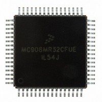
MC908MR32CFUE Freescale Semiconductor, MC908MR32CFUE Datasheet - Page 213

MC908MR32CFUE
Manufacturer Part Number
MC908MR32CFUE
Description
IC MCU 8MHZ 32K FLASH 64-QFP
Manufacturer
Freescale Semiconductor
Series
HC08r
Datasheet
1.MC908MR16CFUE.pdf
(282 pages)
Specifications of MC908MR32CFUE
Core Processor
HC08
Core Size
8-Bit
Speed
8MHz
Connectivity
SCI, SPI
Peripherals
LVD, POR, PWM
Number Of I /o
44
Program Memory Size
32KB (32K x 8)
Program Memory Type
FLASH
Ram Size
768 x 8
Voltage - Supply (vcc/vdd)
4.5 V ~ 5.5 V
Data Converters
A/D 10x10b
Oscillator Type
Internal
Operating Temperature
-40°C ~ 85°C
Package / Case
64-QFP
Processor Series
HC08MR
Core
HC08
Data Bus Width
8 bit
Data Ram Size
768 B
Interface Type
SCI/SPI
Maximum Clock Frequency
8.2 MHz
Number Of Programmable I/os
44
Number Of Timers
6
Operating Supply Voltage
0 V to 5 V
Maximum Operating Temperature
+ 85 C
Mounting Style
SMD/SMT
Development Tools By Supplier
FSICEBASE, M68CBL05CE
Minimum Operating Temperature
- 40 C
On-chip Adc
10-ch x 10-bit
Lead Free Status / RoHS Status
Lead free / RoHS Compliant
Eeprom Size
-
Lead Free Status / Rohs Status
Lead free / RoHS Compliant
Available stocks
Company
Part Number
Manufacturer
Quantity
Price
Company:
Part Number:
MC908MR32CFUE
Manufacturer:
Freescale Semiconductor
Quantity:
10 000
Part Number:
MC908MR32CFUE
Manufacturer:
NXP/恩智浦
Quantity:
20 000
- Current page: 213 of 282
- Download datasheet (2Mb)
OVRF — Overflow Bit
MODF — Mode Fault Bit
SPTE — SPI Transmitter Empty Bit
MODFEN — Mode Fault Enable Bit
SPR1 and SPR0 — SPI Baud Rate Select Bits
Freescale Semiconductor
This clearable, read-only flag is set if software does not read the byte in the receive data register before
the next full byte enters the shift register. In an overflow condition, the byte already in the receive data
register is unaffected, and the byte that shifted in last is lost. Clear the OVRF bit by reading the SPI
status and control register with OVRF set and then reading the receive data register. Reset clears the
OVRF bit.
This clearable, read-only flag is set in a slave SPI if the SS pin goes high during a transmission with
the MODFEN bit set. In a master SPI, the MODF flag is set if the SS pin goes low at any time with the
MODFEN bit set. Clear the MODF bit by reading the SPI status and control register (SPSCR) with
MODF set and then writing to the SPI control register (SPCR). Reset clears the MODF bit.
This clearable, read-only flag is set each time the transmit data register transfers a byte into the shift
register. SPTE generates an SPTE CPU interrupt request or an SPTE DMA service request if the
SPTIE bit in the SPI control register is set also.
For an idle master of idle slave that has no data loaded into its transmit buffer, the SPTE will be set
again within two bus cycles since the transmit buffer empties into the shift register. This allows the user
to queue up a 16-bit value to send. For an already active slave, the load of the shift register cannot
occur until the transmission is completed. This implies that a back-to-back write to the transmit data
register is not possible. The SPTE indicates when the next write can occur.
Reset sets the SPTE bit.
This read/write bit, when set to 1, allows the MODF flag to be set. If the MODF flag is set, clearing the
MODFEN does not clear the MODF flag. If the SPI is enabled as a master and the MODFEN bit is low,
then the SS pin is available as a general-purpose I/O.
If the MODFEN bit is set, then this pin is not available as a general-purpose I/O. When the SPI is
enabled as a slave, the SS pin is not available as a general-purpose I/O regardless of the value of
MODFEN. See
If the MODFEN bit is low, the level of the SS pin does not affect the operation of an enabled SPI
configured as a master. For an enabled SPI configured as a slave, having MODFEN low only prevents
the MODF flag from being set. It does not affect any other part of SPI operation. See
Error.
In master mode, these read/write bits select one of four baud rates as shown in
SPR0 have no effect in slave mode. Reset clears SPR1 and SPR0.
1 = Overflow
0 = No overflow
1 = SS pin at inappropriate logic level
0 = SS pin at appropriate logic level
1 = Transmit data register empty
0 = Transmit data register not empty
Do not write to the SPI data register unless the SPTE bit is high.
15.11.4 SS (Slave
MC68HC908MR32 • MC68HC908MR16 Data Sheet, Rev. 6.1
Select).
NOTE
Table
15.6.2 Mode Fault
15-4. SPR1 and
I/O Registers
213
Related parts for MC908MR32CFUE
Image
Part Number
Description
Manufacturer
Datasheet
Request
R
Part Number:
Description:
Manufacturer:
Freescale Semiconductor, Inc
Datasheet:
Part Number:
Description:
Manufacturer:
Freescale Semiconductor, Inc
Datasheet:
Part Number:
Description:
Manufacturer:
Freescale Semiconductor, Inc
Datasheet:
Part Number:
Description:
Manufacturer:
Freescale Semiconductor, Inc
Datasheet:
Part Number:
Description:
Manufacturer:
Freescale Semiconductor, Inc
Datasheet:
Part Number:
Description:
Manufacturer:
Freescale Semiconductor, Inc
Datasheet:
Part Number:
Description:
Manufacturer:
Freescale Semiconductor, Inc
Datasheet:
Part Number:
Description:
Manufacturer:
Freescale Semiconductor, Inc
Datasheet:
Part Number:
Description:
Manufacturer:
Freescale Semiconductor, Inc
Datasheet:
Part Number:
Description:
Manufacturer:
Freescale Semiconductor, Inc
Datasheet:
Part Number:
Description:
Manufacturer:
Freescale Semiconductor, Inc
Datasheet:
Part Number:
Description:
Manufacturer:
Freescale Semiconductor, Inc
Datasheet:
Part Number:
Description:
Manufacturer:
Freescale Semiconductor, Inc
Datasheet:
Part Number:
Description:
Manufacturer:
Freescale Semiconductor, Inc
Datasheet:
Part Number:
Description:
Manufacturer:
Freescale Semiconductor, Inc
Datasheet:


