MC908MR32CFUE Freescale Semiconductor, MC908MR32CFUE Datasheet - Page 48
MC908MR32CFUE
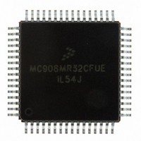
Manufacturer Part Number
MC908MR32CFUE
Description
IC MCU 8MHZ 32K FLASH 64-QFP
Manufacturer
Freescale Semiconductor
Series
HC08r
Datasheet
1.MC908MR16CFUE.pdf
(282 pages)
Specifications of MC908MR32CFUE
Core Processor
HC08
Core Size
8-Bit
Speed
8MHz
Connectivity
SCI, SPI
Peripherals
LVD, POR, PWM
Number Of I /o
44
Program Memory Size
32KB (32K x 8)
Program Memory Type
FLASH
Ram Size
768 x 8
Voltage - Supply (vcc/vdd)
4.5 V ~ 5.5 V
Data Converters
A/D 10x10b
Oscillator Type
Internal
Operating Temperature
-40°C ~ 85°C
Package / Case
64-QFP
Processor Series
HC08MR
Core
HC08
Data Bus Width
8 bit
Data Ram Size
768 B
Interface Type
SCI/SPI
Maximum Clock Frequency
8.2 MHz
Number Of Programmable I/os
44
Number Of Timers
6
Operating Supply Voltage
0 V to 5 V
Maximum Operating Temperature
+ 85 C
Mounting Style
SMD/SMT
Development Tools By Supplier
FSICEBASE, M68CBL05CE
Minimum Operating Temperature
- 40 C
On-chip Adc
10-ch x 10-bit
Lead Free Status / RoHS Status
Lead free / RoHS Compliant
Eeprom Size
-
Lead Free Status / Rohs Status
Lead free / RoHS Compliant
Available stocks
Company
Part Number
Manufacturer
Quantity
Price

Company:
Part Number:
MC908MR32CFUE
Manufacturer:
Freescale Semiconductor
Quantity:
10 000
Part Number:
MC908MR32CFUE
Manufacturer:
NXP/恩智浦
Quantity:
20 000


Analog-to-Digital Converter (ADC)
3.3.3 Conversion Time
Conversion starts after a write to the ADSCR. A conversion is between 16 and 17 ADC clock cycles,
therefore:
The ADC conversion time is determined by the clock source chosen and the divide ratio selected. The
clock source is either the bus clock or CGMXCLK and is selectable by ADICLK located in the ADC clock
register. For example, if CGMXCLK is 4 MHz and is selected as the ADC input clock source, the ADC
input clock divide-by-4 prescale is selected and the CPU bus frequency is 8 MHz:
Since an ADC cycle may be comprised of several bus cycles (eight, 136 minus 128, in the previous
example) and the start of a conversion is initiated by a bus cycle write to the ADSCR, from zero to eight
additional bus cycles may occur before the start of the initial ADC cycle. This results in a fractional ADC
cycle and is represented as the 17th cycle.
3.3.4 Continuous Conversion
In continuous conversion mode, the ADC data registers ADRH and ADRL will be filled with new data after
each conversion. Data from the previous conversion will be overwritten whether that data has been read
or not. Conversions will continue until the ADCO bit is cleared. The COCO bit is set after each conversion
and will stay set until the next read of the ADC data register.
When a conversion is in process and the ADSCR is written, the current conversion data should be
discarded to prevent an incorrect reading.
3.3.5 Result Justification
The conversion result may be formatted in four different ways:
All four of these modes are controlled using MODE0 and MODE1 bits located in the ADC clock register
(ADCR).
Left justification will place the eight most significant bits (MSB) in the corresponding ADC data register
high, ADRH. This may be useful if the result is to be treated as an 8-bit result where the two least
48
1. Left justified
2. Right justified
3. Left Justified sign data mode
4. 8-bit truncation mode
Number of bus cycles = 16 µs x 8 MHz = 128 to 136 cycles
Number of Bus Cycles = Conversion Time x CPU Bus Frequency
Conversion Time =
The ADC frequency must be between f
to meet A/D specifications. See
Characteristics.
Conversion time =
MC68HC908MR32 • MC68HC908MR16 Data Sheet, Rev. 6.1
16 to 17 ADC Cycles
4 MHz/4
16 to17 ADC Cycles
ADC Frequency
19.13 Analog-to-Digital Converter (ADC)
NOTE
= 16 to 17 µs
ADIC
minimum and f
ADIC
maximum
Freescale Semiconductor
Related parts for MC908MR32CFUE
Image
Part Number
Description
Manufacturer
Datasheet
Request
R

Part Number:
Description:
Manufacturer:
Freescale Semiconductor, Inc
Datasheet:
Part Number:
Description:
Manufacturer:
Freescale Semiconductor, Inc
Datasheet:
Part Number:
Description:
Manufacturer:
Freescale Semiconductor, Inc
Datasheet:
Part Number:
Description:
Manufacturer:
Freescale Semiconductor, Inc
Datasheet:
Part Number:
Description:
Manufacturer:
Freescale Semiconductor, Inc
Datasheet:
Part Number:
Description:
Manufacturer:
Freescale Semiconductor, Inc
Datasheet:
Part Number:
Description:
Manufacturer:
Freescale Semiconductor, Inc
Datasheet:
Part Number:
Description:
Manufacturer:
Freescale Semiconductor, Inc
Datasheet:
Part Number:
Description:
Manufacturer:
Freescale Semiconductor, Inc
Datasheet:
Part Number:
Description:
Manufacturer:
Freescale Semiconductor, Inc
Datasheet:
Part Number:
Description:
Manufacturer:
Freescale Semiconductor, Inc
Datasheet:
Part Number:
Description:
Manufacturer:
Freescale Semiconductor, Inc
Datasheet:
Part Number:
Description:
Manufacturer:
Freescale Semiconductor, Inc
Datasheet:
Part Number:
Description:
Manufacturer:
Freescale Semiconductor, Inc
Datasheet:
Part Number:
Description:
Manufacturer:
Freescale Semiconductor, Inc
Datasheet: