HD64F2612FA20 Renesas Electronics America, HD64F2612FA20 Datasheet - Page 34
HD64F2612FA20
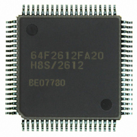
Manufacturer Part Number
HD64F2612FA20
Description
IC H8S MCU FLASH 128K 80QFP
Manufacturer
Renesas Electronics America
Series
H8® H8S/2600r
Specifications of HD64F2612FA20
Core Processor
H8S/2600
Core Size
16-Bit
Speed
20MHz
Connectivity
CAN, SCI
Peripherals
POR, PWM, WDT
Number Of I /o
43
Program Memory Size
128KB (128K x 8)
Program Memory Type
FLASH
Ram Size
4K x 8
Voltage - Supply (vcc/vdd)
4.5 V ~ 5.5 V
Data Converters
A/D 12x10b
Oscillator Type
Internal
Operating Temperature
-20°C ~ 75°C
Package / Case
80-QFP
Lead Free Status / RoHS Status
Contains lead / RoHS non-compliant
Eeprom Size
-
Available stocks
Company
Part Number
Manufacturer
Quantity
Price

Part Number:
HD64F2612FA20
Manufacturer:
RENESAS/瑞萨
Quantity:
20 000
Part Number:
HD64F2612FA20J
Manufacturer:
RENESAS/瑞萨
Quantity:
20 000


Table 14.5
Table 14.6
Table 14.7
Table 14.8
Table 14.9
Table 14.10 Serial Transfer Formats (Asynchronous Mode) ...................................................... 339
Table 14.11 SSR Status Flags and Receive Data Handling......................................................... 346
Table 14.12 SCI Interrupt Sources .............................................................................................. 375
Table 14.13 SCI Interrupt Sources .............................................................................................. 376
Section 15 Controller Area Network (HCAN)
Table 15.1
Table 15.2
Table 15.3
Table 15.4
Table 15.5
Section 16 A/D Converter
Table 16.1
Table 16.2
Table 16.3
Table 16.4
Table 16.5
Table 16.6
Section 18 ROM
Table 18.1
Table 18.2
Table 18.3
Table 18.4
Table 18.5
Table 18.6
Table 18.7
Section 19 Clock Pulse Generator
Table 19.1
Table 19.2
Table 19.3
Rev. 7.00 Sep. 11, 2009 Page xxxii of xxxiv
REJ09B0211-0700
Maximum Bit Rate with External Clock Input (Asynchronous Mode)................... 335
BRR Settings for Various Bit Rates (Clocked Synchronous Mode) ....................... 336
Maximum Bit Rate with External Clock Input (Clocked Synchronous Mode)....... 336
Examples of Bit Rate for Various BRR Settings (Smart Card Interface Mode)
(When n = 0 and S = 372) ....................................................................................... 337
Maximum Bit Rate at Various Frequencies (Smart Card Interface Mode)
(When S = 372) ....................................................................................................... 337
HCAN Pins.............................................................................................................. 385
Limits for Settable Value ........................................................................................ 415
Setting Range for TSEG1 and TSEG2 in BCR ....................................................... 416
HCAN Interrupt Sources ......................................................................................... 428
Interval Limitation between TXPR and TXPR or between TXPR and TXCR ....... 433
Pin Configuration .................................................................................................... 437
Analog Input Channels and Corresponding ADDR Registers................................. 439
A/D Conversion Time (Single Mode) ..................................................................... 444
A/D Conversion Time (Scan Mode)........................................................................ 444
A/D Converter Interrupt Source .............................................................................. 445
Analog Pin Specifications ....................................................................................... 450
Differences between Boot Mode and User Program Mode..................................... 455
Pin Configuration .................................................................................................... 459
Setting On-Board Programming Modes.................................................................. 463
Boot Mode Operation.............................................................................................. 465
System Clock Frequencies for Which Automatic Adjustment of LSI Bit Rate Is
Possible ................................................................................................................... 465
Flash Memory Operating States .............................................................................. 475
Registers Present in F-ZTAT Version but Absent in Mask ROM Version ............. 476
Damping Resistance Value ..................................................................................... 480
Crystal Resonator Characteristics............................................................................ 481
External Clock Input Conditions ............................................................................. 482
Related parts for HD64F2612FA20
Image
Part Number
Description
Manufacturer
Datasheet
Request
R


Part Number:
Description:
KIT STARTER FOR M16C/29
Manufacturer:
Renesas Electronics America
Datasheet:

Part Number:
Description:
KIT STARTER FOR R8C/2D
Manufacturer:
Renesas Electronics America
Datasheet:

Part Number:
Description:
R0K33062P STARTER KIT
Manufacturer:
Renesas Electronics America
Datasheet:

Part Number:
Description:
KIT STARTER FOR R8C/23 E8A
Manufacturer:
Renesas Electronics America
Datasheet:

Part Number:
Description:
KIT STARTER FOR R8C/25
Manufacturer:
Renesas Electronics America
Datasheet:

Part Number:
Description:
KIT STARTER H8S2456 SHARPE DSPLY
Manufacturer:
Renesas Electronics America
Datasheet:

Part Number:
Description:
KIT STARTER FOR R8C38C
Manufacturer:
Renesas Electronics America
Datasheet:

Part Number:
Description:
KIT STARTER FOR R8C35C
Manufacturer:
Renesas Electronics America
Datasheet:

Part Number:
Description:
KIT STARTER FOR R8CL3AC+LCD APPS
Manufacturer:
Renesas Electronics America
Datasheet:
Part Number:
Description:
KIT STARTER FOR RX610
Manufacturer:
Renesas Electronics America
Datasheet:

Part Number:
Description:
KIT STARTER FOR R32C/118
Manufacturer:
Renesas Electronics America
Datasheet:

Part Number:
Description:
KIT DEV RSK-R8C/26-29
Manufacturer:
Renesas Electronics America
Datasheet:

Part Number:
Description:
KIT STARTER FOR SH7124
Manufacturer:
Renesas Electronics America
Datasheet:

Part Number:
Description:
KIT STARTER FOR H8SX/1622
Manufacturer:
Renesas Electronics America
Datasheet: