HD64F2612FA20 Renesas Electronics America, HD64F2612FA20 Datasheet - Page 392
HD64F2612FA20
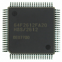
Manufacturer Part Number
HD64F2612FA20
Description
IC H8S MCU FLASH 128K 80QFP
Manufacturer
Renesas Electronics America
Series
H8® H8S/2600r
Specifications of HD64F2612FA20
Core Processor
H8S/2600
Core Size
16-Bit
Speed
20MHz
Connectivity
CAN, SCI
Peripherals
POR, PWM, WDT
Number Of I /o
43
Program Memory Size
128KB (128K x 8)
Program Memory Type
FLASH
Ram Size
4K x 8
Voltage - Supply (vcc/vdd)
4.5 V ~ 5.5 V
Data Converters
A/D 12x10b
Oscillator Type
Internal
Operating Temperature
-20°C ~ 75°C
Package / Case
80-QFP
Lead Free Status / RoHS Status
Contains lead / RoHS non-compliant
Eeprom Size
-
Available stocks
Company
Part Number
Manufacturer
Quantity
Price

Part Number:
HD64F2612FA20
Manufacturer:
RENESAS/瑞萨
Quantity:
20 000
Part Number:
HD64F2612FA20J
Manufacturer:
RENESAS/瑞萨
Quantity:
20 000


Section 14 Serial Communication Interface (SCI)
14.6.2
Before transmitting and receiving data, the TE and RE bits in SCR should be cleared to 0, then the
SCI should be initialized as described in a sample flowchart in figure 14.15. When the operating
mode, or transfer format, is changed for example, the TE and RE bits must be cleared to 0 before
making the change using the following procedure. When the TE bit is cleared to 0, the TDRE flag
is set to 1. Note that clearing the RE bit to 0 does not change the contents of the RDRF, PER,
FER, and ORER flags, or the contents of RDR.
Rev. 7.00 Sep. 11, 2009 Page 356 of 566
REJ09B0211-0700
Note: In simultaneous transmit and receive operations, the TE and RE bits should both be cleared
Set TE and RE bits in SCR to 1, and
SCI Initialization (Clocked Synchronous Mode)
set RIE, TIE, TEIE, and MPIE bits
Clear TE and RE bits in SCR to 0
Set CKE1 and CKE0 bits in SCR
to 0 or set to 1 simultaneously.
Set data transfer format in
1-bit interval elapsed?
Set value in BRR
Start initialization
SMR and SCMR
<Transfer start>
(TE, RE bits 0)
Figure 14.15 Sample SCI Initialization Flowchart
Yes
Wait
No
[4]
[2]
[3]
[1]
[1] Set the clock selection in SCR. Be sure
[2] Set the data transfer format in SMR and
[3] Write a value corresponding to the bit
[4] Wait at least one bit interval, then set
to clear bits RIE, TIE, TEIE, and MPIE,
TE and RE, to 0.
SCMR.
rate to BRR. Not necessary if an
external clock is used.
the TE bit or RE bit in SCR to 1.
Also set the RIE, TIE TEIE, and MPIE
bits.
Setting the TE and RE bits enables the
TxD and RxD pins to be used.
Related parts for HD64F2612FA20
Image
Part Number
Description
Manufacturer
Datasheet
Request
R


Part Number:
Description:
KIT STARTER FOR M16C/29
Manufacturer:
Renesas Electronics America
Datasheet:

Part Number:
Description:
KIT STARTER FOR R8C/2D
Manufacturer:
Renesas Electronics America
Datasheet:

Part Number:
Description:
R0K33062P STARTER KIT
Manufacturer:
Renesas Electronics America
Datasheet:

Part Number:
Description:
KIT STARTER FOR R8C/23 E8A
Manufacturer:
Renesas Electronics America
Datasheet:

Part Number:
Description:
KIT STARTER FOR R8C/25
Manufacturer:
Renesas Electronics America
Datasheet:

Part Number:
Description:
KIT STARTER H8S2456 SHARPE DSPLY
Manufacturer:
Renesas Electronics America
Datasheet:

Part Number:
Description:
KIT STARTER FOR R8C38C
Manufacturer:
Renesas Electronics America
Datasheet:

Part Number:
Description:
KIT STARTER FOR R8C35C
Manufacturer:
Renesas Electronics America
Datasheet:

Part Number:
Description:
KIT STARTER FOR R8CL3AC+LCD APPS
Manufacturer:
Renesas Electronics America
Datasheet:
Part Number:
Description:
KIT STARTER FOR RX610
Manufacturer:
Renesas Electronics America
Datasheet:

Part Number:
Description:
KIT STARTER FOR R32C/118
Manufacturer:
Renesas Electronics America
Datasheet:

Part Number:
Description:
KIT DEV RSK-R8C/26-29
Manufacturer:
Renesas Electronics America
Datasheet:

Part Number:
Description:
KIT STARTER FOR SH7124
Manufacturer:
Renesas Electronics America
Datasheet:

Part Number:
Description:
KIT STARTER FOR H8SX/1622
Manufacturer:
Renesas Electronics America
Datasheet: