DF2265TE13V Renesas Electronics America, DF2265TE13V Datasheet - Page 444
DF2265TE13V
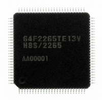
Manufacturer Part Number
DF2265TE13V
Description
IC H8S/2265 MCU FLASH 100TQFP
Manufacturer
Renesas Electronics America
Series
H8® H8S/2200r
Specifications of DF2265TE13V
Core Processor
H8S/2000
Core Size
16-Bit
Speed
13MHz
Connectivity
I²C, SCI, SmartCard
Peripherals
LCD, POR, PWM, WDT
Number Of I /o
67
Program Memory Size
128KB (128K x 8)
Program Memory Type
FLASH
Ram Size
4K x 8
Voltage - Supply (vcc/vdd)
3 V ~ 5.5 V
Data Converters
A/D 10x10b, D/A 2x8b
Oscillator Type
Internal
Operating Temperature
-20°C ~ 75°C
Package / Case
100-TQFP, 100-VQFP
Lead Free Status / RoHS Status
Lead free / RoHS Compliant
Eeprom Size
-
Available stocks
Company
Part Number
Manufacturer
Quantity
Price
Company:

Part Number:
DF2265TE13V
Manufacturer:
Renesas Electronics America
Quantity:
10 000


Section 14 I
Rev. 5.00 Sep. 01, 2009 Page 392 of 656
REJ09B0071-0500
5
4
3
Bit
2
1
0
Bit Name
CKS2
CKS1
CKS0
BC2
BC1
BC0
2
C Bus Interface (IIC) (Supported as an Option by H8S/2264 Group)
Initial
Value
0
0
0
0
0
0
R/W
R/W
R/W
R/W
R/W
R/W
R/W
Description
Serial Clock Select 2 to 0
This bit is valid only in master mode.
These bits select the required transfer rate, together with
the IICX 1 and IICX0 bit in SCRX. Refer table 14.3.
Bit Counter 2 to 0
These bits specify the number of bits to be transferred
next. With the I
one addition acknowledge bit. Bit BC2 to BC0 settings
should be made during an interval between transfer
frames. If bits BC2 to BC0 are set to a value other than
000, the setting should be made while the SCL line is low.
The value returns to 000 at the end of a data transfer,
including the acknowledge bit.
I
000: 9 bit
001: 2 bit
010: 3 bit
011: 4 bit
100: 5 bit
101: 6 bit
110: 7 bit
111: 8 bit
2
C Bus Format
2
C bus format, the data is transferred with
Clocked Synchronous Mode
000: 8 bit
001: 1 bit
010: 2 bit
011: 3 bit
100: 4 bit
101: 5 bit
110: 6 bit
111: 7 bit
Related parts for DF2265TE13V
Image
Part Number
Description
Manufacturer
Datasheet
Request
R

Part Number:
Description:
CONN SOCKET 2POS 7.92MM WHITE
Manufacturer:
Hirose Electric Co Ltd
Datasheet:

Part Number:
Description:
CONN SOCKET 4POS 7.92MM WHITE
Manufacturer:
Hirose Electric Co Ltd
Datasheet:

Part Number:
Description:
CONN SOCKET 5POS 7.92MM WHITE
Manufacturer:
Hirose Electric Co Ltd
Datasheet:

Part Number:
Description:
CONN SOCKET 3POS 7.92MM WHITE
Manufacturer:
Hirose Electric Co Ltd
Datasheet:
Part Number:
Description:
CONN SOCKET 5POS 7.92MM WHITE
Manufacturer:
Hirose Electric Co Ltd
Datasheet:

Part Number:
Description:
CONN SOCKET 2POS 7.92MM WHITE
Manufacturer:
Hirose Electric Co Ltd
Datasheet:
Part Number:
Description:
CONN SOCKET 3POS 7.92MM WHITE
Manufacturer:
Hirose Electric Co Ltd
Datasheet:
Part Number:
Description:
CONN SOCKET 4POS 7.92MM WHITE
Manufacturer:
Hirose Electric Co Ltd
Datasheet:

Part Number:
Description:
CONN HEADER 2POS 7.92MM R/A TIN
Manufacturer:
Hirose Electric Co Ltd
Datasheet:

Part Number:
Description:
CONN HEADER 4POS 7.92MM R/A TIN
Manufacturer:
Hirose Electric Co Ltd
Datasheet:

Part Number:
Description:
KIT STARTER FOR M16C/29
Manufacturer:
Renesas Electronics America
Datasheet:

Part Number:
Description:
KIT STARTER FOR R8C/2D
Manufacturer:
Renesas Electronics America
Datasheet:

Part Number:
Description:
R0K33062P STARTER KIT
Manufacturer:
Renesas Electronics America
Datasheet:

Part Number:
Description:
KIT STARTER FOR R8C/23 E8A
Manufacturer:
Renesas Electronics America
Datasheet:

Part Number:
Description:
KIT STARTER FOR R8C/25
Manufacturer:
Renesas Electronics America
Datasheet: