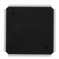
HD64F7145F50 Renesas Electronics America, HD64F7145F50 Datasheet - Page 549

HD64F7145F50
Manufacturer Part Number
HD64F7145F50
Description
IC SUPERH MCU FLASH 256K FP144F
Manufacturer
Renesas Electronics America
Series
SuperH® SH7144r
Datasheet
1.HD64F7144F50V.pdf
(932 pages)
Specifications of HD64F7145F50
Core Processor
SH-2
Core Size
32-Bit
Speed
50MHz
Connectivity
EBI/EMI, I²C, SCI
Peripherals
DMA, POR, PWM, WDT
Number Of I /o
98
Program Memory Size
256KB (256K x 8)
Program Memory Type
FLASH
Ram Size
8K x 8
Voltage - Supply (vcc/vdd)
3 V ~ 3.6 V
Data Converters
A/D 8x10b
Oscillator Type
Internal
Operating Temperature
-20°C ~ 75°C
Package / Case
144-LQFP
Lead Free Status / RoHS Status
Contains lead / RoHS non-compliant
Eeprom Size
-
Available stocks
Company
Part Number
Manufacturer
Quantity
Price
Part Number:
HD64F7145F50
Manufacturer:
RENESAS/瑞萨
Quantity:
20 000
Company:
Part Number:
HD64F7145F50V
Manufacturer:
Renesas Electronics America
Quantity:
10 000
Part Number:
HD64F7145F50V
Manufacturer:
RENESAS/瑞萨
Quantity:
20 000
- Current page: 549 of 932
- Download datasheet (6Mb)
The following description gives the procedures for and operations of receiving data in one byte
units by fixing SCL low for every data reception using the HNDS bit function.
1. Clear the TRS bit in ICCR to 0 to change from the transmit mode to the receive mode.
2. When ICDR is read (a dummy read operation), the receiving of data starts; the receive clock is
3. The master device sets SDA to low on the 9th cycle of the receive clock and returns the
4. To identify the next interrupt, the IRIC flag is cleared to 0.
5. Read the receive data of ICDR. This clears the ICDRF flag to 0, and the master devise outputs
6. Set the ACKB bit to 1 (setting of acknowledge data for the final reception).
7. Read ICDR receive data. This clears the ICDRF flag to 0. The master device outputs the
8. When one frame of data has been received, the ICDRF, IRIC, and IRTR flags are set to 1 at the
9. Clear the IRIC flag to 0.
10. Read ICDR receives data after setting the TRS bit to 1. This clears the ICDRF flag to 0.
11. Write 0 to BBSY and SCP in ICCR to generate the stop condition.
Clear the ACKB bit in ICSR to 0 (setting of the acknowledge data).
Set the HNDS bit in SCRX to 1.
Clear the IRIC flag to 0 to confirm that reception has been completed.
When the first frame is the final receive data, perform end processing in step 6 and subsequent
steps.
output in synchronization with the internal clock, and the first datum is then received. (Data of
the SDA pin is stored in ICDRS in synchronization with the rising edge of receive clock.)
acknowledge bit. The receive data is transferred from ICDRS to ICDRR at the rising edge of
the 9th cycle of the receive clock, and the ICDRF, IRIC, and IRTR flags are set to 1. When the
IEIC bit in ICCR has been set to 1, an interrupt request is generated for the CPU. The master
devise fixes SCL low between at the falling edge of 9th cycle of the receive clock and read of
ICDR data.
When the next frame is the final receive data, perform end processing in step 6 and subsequent
steps.
the receive clock continuously for the reception of the next data.
Data can be received by repeating the steps 3 to 5.
receive clock to receive data.
rising edge of the 9th cycle of receive clock.
This changes SDA from low to high when SCL is high, and generates the stop condition.
Rev.4.00 Mar. 27, 2008 Page 503 of 882
14. I
2
C Bus Interface (IIC) Option
REJ09B0108-0400
Related parts for HD64F7145F50
Image
Part Number
Description
Manufacturer
Datasheet
Request
R

Part Number:
Description:
KIT STARTER FOR M16C/29
Manufacturer:
Renesas Electronics America
Datasheet:

Part Number:
Description:
KIT STARTER FOR R8C/2D
Manufacturer:
Renesas Electronics America
Datasheet:

Part Number:
Description:
R0K33062P STARTER KIT
Manufacturer:
Renesas Electronics America
Datasheet:

Part Number:
Description:
KIT STARTER FOR R8C/23 E8A
Manufacturer:
Renesas Electronics America
Datasheet:

Part Number:
Description:
KIT STARTER FOR R8C/25
Manufacturer:
Renesas Electronics America
Datasheet:

Part Number:
Description:
KIT STARTER H8S2456 SHARPE DSPLY
Manufacturer:
Renesas Electronics America
Datasheet:

Part Number:
Description:
KIT STARTER FOR R8C38C
Manufacturer:
Renesas Electronics America
Datasheet:

Part Number:
Description:
KIT STARTER FOR R8C35C
Manufacturer:
Renesas Electronics America
Datasheet:

Part Number:
Description:
KIT STARTER FOR R8CL3AC+LCD APPS
Manufacturer:
Renesas Electronics America
Datasheet:

Part Number:
Description:
KIT STARTER FOR RX610
Manufacturer:
Renesas Electronics America
Datasheet:

Part Number:
Description:
KIT STARTER FOR R32C/118
Manufacturer:
Renesas Electronics America
Datasheet:

Part Number:
Description:
KIT DEV RSK-R8C/26-29
Manufacturer:
Renesas Electronics America
Datasheet:

Part Number:
Description:
KIT STARTER FOR SH7124
Manufacturer:
Renesas Electronics America
Datasheet:

Part Number:
Description:
KIT STARTER FOR H8SX/1622
Manufacturer:
Renesas Electronics America
Datasheet:


