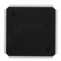
HD64F7145F50 Renesas Electronics America, HD64F7145F50 Datasheet - Page 741

HD64F7145F50
Manufacturer Part Number
HD64F7145F50
Description
IC SUPERH MCU FLASH 256K FP144F
Manufacturer
Renesas Electronics America
Series
SuperH® SH7144r
Datasheet
1.HD64F7144F50V.pdf
(932 pages)
Specifications of HD64F7145F50
Core Processor
SH-2
Core Size
32-Bit
Speed
50MHz
Connectivity
EBI/EMI, I²C, SCI
Peripherals
DMA, POR, PWM, WDT
Number Of I /o
98
Program Memory Size
256KB (256K x 8)
Program Memory Type
FLASH
Ram Size
8K x 8
Voltage - Supply (vcc/vdd)
3 V ~ 3.6 V
Data Converters
A/D 8x10b
Oscillator Type
Internal
Operating Temperature
-20°C ~ 75°C
Package / Case
144-LQFP
Lead Free Status / RoHS Status
Contains lead / RoHS non-compliant
Eeprom Size
-
Available stocks
Company
Part Number
Manufacturer
Quantity
Price
Part Number:
HD64F7145F50
Manufacturer:
RENESAS/瑞萨
Quantity:
20 000
Company:
Part Number:
HD64F7145F50V
Manufacturer:
Renesas Electronics America
Quantity:
10 000
Part Number:
HD64F7145F50V
Manufacturer:
RENESAS/瑞萨
Quantity:
20 000
- Current page: 741 of 932
- Download datasheet (6Mb)
22.2
Table 22.1 shows the H-UDI pin configuration.
Table 22.1 H-UDI Pins
Pin Name
Test clock
Test mode
select
Test data
input
Test data
output
Test reset
Input/Output Pins
Abbreviation
TCK
TMS
TDI
TDO
TRST
Input
Input
Input
Output
Input
I/O
TCK supplies an independent clock to the H-UDI. As
the clock input to TCK is supplied directly to the H-UDI,
a clock waveform with a duty cycle close to 50%
should be input (see section 26, Electrical
Characteristics, for details).
Test Mode Select Input Signal
TMS is sampled at the rising edge of TCK. TMS
controls the internal state of the TAP controller.
Serial Data Input
TDI performs serial input of instructions and data to H-
UDI registers. TDI is sampled at the rising edge of
TCK.
Serial Data Output
TDO performs serial output of instructions and data
from H-UDI registers. Transfer is synchronized with
TCK. When no signal is being output, TDO goes to the
high-impedance state.
Test Reset Input Signal
TRST is used to initialize the H-UDI asynchronously.
Function
Test Clock Input
Rev.4.00 Mar. 27, 2008 Page 695 of 882
22. User Debugging Interface (H-UDI)
REJ09B0108-0400
Related parts for HD64F7145F50
Image
Part Number
Description
Manufacturer
Datasheet
Request
R

Part Number:
Description:
KIT STARTER FOR M16C/29
Manufacturer:
Renesas Electronics America
Datasheet:

Part Number:
Description:
KIT STARTER FOR R8C/2D
Manufacturer:
Renesas Electronics America
Datasheet:

Part Number:
Description:
R0K33062P STARTER KIT
Manufacturer:
Renesas Electronics America
Datasheet:

Part Number:
Description:
KIT STARTER FOR R8C/23 E8A
Manufacturer:
Renesas Electronics America
Datasheet:

Part Number:
Description:
KIT STARTER FOR R8C/25
Manufacturer:
Renesas Electronics America
Datasheet:

Part Number:
Description:
KIT STARTER H8S2456 SHARPE DSPLY
Manufacturer:
Renesas Electronics America
Datasheet:

Part Number:
Description:
KIT STARTER FOR R8C38C
Manufacturer:
Renesas Electronics America
Datasheet:

Part Number:
Description:
KIT STARTER FOR R8C35C
Manufacturer:
Renesas Electronics America
Datasheet:

Part Number:
Description:
KIT STARTER FOR R8CL3AC+LCD APPS
Manufacturer:
Renesas Electronics America
Datasheet:

Part Number:
Description:
KIT STARTER FOR RX610
Manufacturer:
Renesas Electronics America
Datasheet:

Part Number:
Description:
KIT STARTER FOR R32C/118
Manufacturer:
Renesas Electronics America
Datasheet:

Part Number:
Description:
KIT DEV RSK-R8C/26-29
Manufacturer:
Renesas Electronics America
Datasheet:

Part Number:
Description:
KIT STARTER FOR SH7124
Manufacturer:
Renesas Electronics America
Datasheet:

Part Number:
Description:
KIT STARTER FOR H8SX/1622
Manufacturer:
Renesas Electronics America
Datasheet:


