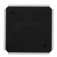
HD64F7145F50 Renesas Electronics America, HD64F7145F50 Datasheet - Page 711

HD64F7145F50
Manufacturer Part Number
HD64F7145F50
Description
IC SUPERH MCU FLASH 256K FP144F
Manufacturer
Renesas Electronics America
Series
SuperH® SH7144r
Datasheet
1.HD64F7144F50V.pdf
(932 pages)
Specifications of HD64F7145F50
Core Processor
SH-2
Core Size
32-Bit
Speed
50MHz
Connectivity
EBI/EMI, I²C, SCI
Peripherals
DMA, POR, PWM, WDT
Number Of I /o
98
Program Memory Size
256KB (256K x 8)
Program Memory Type
FLASH
Ram Size
8K x 8
Voltage - Supply (vcc/vdd)
3 V ~ 3.6 V
Data Converters
A/D 8x10b
Oscillator Type
Internal
Operating Temperature
-20°C ~ 75°C
Package / Case
144-LQFP
Lead Free Status / RoHS Status
Contains lead / RoHS non-compliant
Eeprom Size
-
Available stocks
Company
Part Number
Manufacturer
Quantity
Price
Part Number:
HD64F7145F50
Manufacturer:
RENESAS/瑞萨
Quantity:
20 000
Company:
Part Number:
HD64F7145F50V
Manufacturer:
Renesas Electronics America
Quantity:
10 000
Part Number:
HD64F7145F50V
Manufacturer:
RENESAS/瑞萨
Quantity:
20 000
- Current page: 711 of 932
- Download datasheet (6Mb)
19.5
The flash memory has the following registers. For details on register addresses and register states
during each processing, refer to section 25, List of Registers.
• Flash memory control register 1 (FLMCR1)
• Flash memory control register 2 (FLMCR2)
• Erase block register 1 (EBR1)
• Erase block register 2 (EBR2)
• RAM emulation register (RAMER)
19.5.1
FLMCR1 is a register that makes the flash memory change to program mode, program-verify
mode, erase mode, or erase-verify mode. For details on register setting, refer to section 19.8, Flash
Memory Programming/Erasing.
Bit
7
6
5
4
Bit Name
FEW
SWE
ESU
PSU
Register Descriptions
Flash Memory Control Register 1 (FLMCR1)
Initial Value
1/0
0
0
0
R/W
R
R/W
R/W
R/W
Description
Flash Write Enable*
Reflects the input level at the FWP pin. It is set to 1
when a low level is input to the FWP pin, and cleared
to 0 when a high level is input.
Software Write Enable
When this bit is set to 1 while the FEW bit is 1, flash
memory programming/erasing is enabled. When this
bit is cleared to 0, other FLMCR1 bits and all EBR1
and EBR2 bits cannot be set.
Erase Setup
When this bit is set to 1 while the FEW and SWE bits
are 1, the flash memory changes to the erase setup
state. When it is cleared to 0, the erase setup state is
cancelled.
Program Setup
When this bit is set to 1 while the FEW and SWE bits
are 1, the flash memory changes to the program
setup state. When it is cleared to 0, the program
setup state is cancelled.
Rev.4.00 Mar. 27, 2008 Page 665 of 882
19. Flash Memory (F-ZTAT Version)
REJ09B0108-0400
Related parts for HD64F7145F50
Image
Part Number
Description
Manufacturer
Datasheet
Request
R

Part Number:
Description:
KIT STARTER FOR M16C/29
Manufacturer:
Renesas Electronics America
Datasheet:

Part Number:
Description:
KIT STARTER FOR R8C/2D
Manufacturer:
Renesas Electronics America
Datasheet:

Part Number:
Description:
R0K33062P STARTER KIT
Manufacturer:
Renesas Electronics America
Datasheet:

Part Number:
Description:
KIT STARTER FOR R8C/23 E8A
Manufacturer:
Renesas Electronics America
Datasheet:

Part Number:
Description:
KIT STARTER FOR R8C/25
Manufacturer:
Renesas Electronics America
Datasheet:

Part Number:
Description:
KIT STARTER H8S2456 SHARPE DSPLY
Manufacturer:
Renesas Electronics America
Datasheet:

Part Number:
Description:
KIT STARTER FOR R8C38C
Manufacturer:
Renesas Electronics America
Datasheet:

Part Number:
Description:
KIT STARTER FOR R8C35C
Manufacturer:
Renesas Electronics America
Datasheet:

Part Number:
Description:
KIT STARTER FOR R8CL3AC+LCD APPS
Manufacturer:
Renesas Electronics America
Datasheet:

Part Number:
Description:
KIT STARTER FOR RX610
Manufacturer:
Renesas Electronics America
Datasheet:

Part Number:
Description:
KIT STARTER FOR R32C/118
Manufacturer:
Renesas Electronics America
Datasheet:

Part Number:
Description:
KIT DEV RSK-R8C/26-29
Manufacturer:
Renesas Electronics America
Datasheet:

Part Number:
Description:
KIT STARTER FOR SH7124
Manufacturer:
Renesas Electronics America
Datasheet:

Part Number:
Description:
KIT STARTER FOR H8SX/1622
Manufacturer:
Renesas Electronics America
Datasheet:


