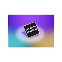
XR17D152CM-F Exar Corporation, XR17D152CM-F Datasheet - Page 33

XR17D152CM-F
Manufacturer Part Number
XR17D152CM-F
Description
IC UART PCI BUS DUAL 100TQFP
Manufacturer
Exar Corporation
Type
RS- 232 or RS- 422 or RS- 485r
Datasheet
1.XR17D152CM-F.pdf
(68 pages)
Specifications of XR17D152CM-F
Number Of Channels
2, DUART
Package / Case
100-TQFP
Features
*
Fifo's
64 Byte
Protocol
RS485
Voltage - Supply
3.3V, 5V
With Auto Flow Control
Yes
With Irda Encoder/decoder
Yes
With False Start Bit Detection
Yes
With Modem Control
Yes
Mounting Type
Surface Mount
Data Rate
6.25 Mbps
Supply Voltage (max)
5.25 V or 5.5 V
Supply Voltage (min)
4.5 V or 4.75 V
Supply Current
4 mA
Maximum Operating Temperature
+ 70 C
Minimum Operating Temperature
0 C
Mounting Style
SMD/SMT
Operating Supply Voltage
5 V
No. Of Channels
2
Uart Features
Tx/Rx FIFO Counters
Supply Voltage Range
3V To 5.5V
Operating Temperature Range
0°C To +70°C
Digital Ic Case Style
TQFP
No. Of Pins
100
Rohs Compliant
Yes
Lead Free Status / RoHS Status
Lead free / RoHS Compliant
Lead Free Status / RoHS Status
Lead free / RoHS Compliant, Lead free / RoHS Compliant
Other names
1016-1288
Available stocks
Company
Part Number
Manufacturer
Quantity
Price
Company:
Part Number:
XR17D152CM-F
Manufacturer:
EXAR
Quantity:
520
Company:
Part Number:
XR17D152CM-F
Manufacturer:
Exar Corporation
Quantity:
10 000
Part Number:
XR17D152CM-F
Manufacturer:
EXAR/艾科嘉
Quantity:
20 000
áç
áç
áç
áç
REV. 1.2.0
Each UART channel provides an internal loopback capability for system diagnostic. The internal loopback
mode is enabled by setting MCR register bit-4 to logic 1. All regular UART functions operate normally.
Figure 18
output is internally routed to the receive shift register input allowing the system to receive the same data that it
was sending. The TX, RTS# and DTR# pins are held HIGH (idle or de-asserted state), and the CTS#, DSR#
CD# and RI# inputs are ignored.
The 2 sets of UART configuration registers are decoded using address lines A9 to A11 as shown below.
5.6
5.7
Internal Loopback
UART CHANNEL CONFIGURATION REGISTERS AND ADDRESS DECODING.
shows how the modem port signals are re-configured. Transmit data from the transmit shift register
F
IGURE
18. I
NTERNAL
L
OOP
A11
0
0
B
ACK
Transmit Shift
Receive Shift
F
A10
Register
Register
UNCTION IN EACH
0
0
A9
33
DTR#
DSR#
RTS#
CTS#
0
1
CD#
RI#
MCR bit-4=1
UNIVERSAL (3.3V AND 5V) PCI BUS DUAL UART
UART C
OP1#
OP2#
S
VCC
VCC
UART C
ELECTION
VCC
0
1
HANNEL
HANNEL
RX [1:0]
TX [1:0]
RTS# [1:0]
CTS# [1:0]
DTR# [1:0]
DSR# [1:0]
RI# [1:0]
CD# [1:0]
XR17D152


