IAR-KSK-IMX25 Freescale Semiconductor, IAR-KSK-IMX25 Datasheet - Page 42
IAR-KSK-IMX25
Manufacturer Part Number
IAR-KSK-IMX25
Description
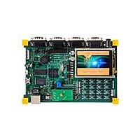
KIT DEVELOPMENT I.MX257, ARM926
Manufacturer
Freescale Semiconductor
Series
i.MX25r
Type
MCUr
Datasheets
1.MCIMX25WPDKJ.pdf
(2 pages)
2.IAR-KSK-IMX25.pdf
(154 pages)
3.IAR-KSK-IMX25.pdf
(2 pages)
4.IAR-KSK-IMX25.pdf
(57 pages)
Specifications of IAR-KSK-IMX25
Contents
Board, Cables, CD, Debugger, Power Supply
Processor To Be Evaluated
I.MX257
Processor Series
i.MX25
Data Bus Width
16 bit
Interface Type
UART, JTAG, USB, Ethernet, SD/MMC
Core
ARM926EJ-S
Silicon Manufacturer
Freescale
Core Architecture
ARM
Core Sub-architecture
ARM9
Silicon Core Number
I.MX2
Silicon Family Name
I.MX25
Mcu Supported Families
I.MX25
For Use With/related Products
i.MX25
Lead Free Status / RoHS Status
Lead free / RoHS Compliant


2. Minimum condition for tps: wcs model, 1.1 V, I/O 1.7 V, and 105 °C. tps is measured between VIL to VIH for rising edge and
3. Maximum condition for tdit: bcs model, 1.3 V, I/O 1.9 V, and –40 °C.
4. Maximum condition for tpi and trfi: wcs model, 1.1 V, I/O 1.7 V and 105 °C. Minimum condition for tpi and trfi: bcs model, 1.3 V,
Table 31
3.7
This section contains the timing and electrical parameters for i.MX25 modules.
3.7.1
Figure 7
42
1
2
3
4
AC input logic high
AC input logic low
AC differential input voltage
AC differential cross point voltage for input
AC differential cross point voltage for output
between VIH to VIL for falling edge.
I/O 1.9 V and –40 °C. Input transition time from pad is 5 ns (20%–80%).
Note that the Jedec SSTL_18 specification (JESD8-15a) for an SSTL interface for class II operation supersedes any
specification in this document.
Vid(ac) specifies the input differential voltage |Vtr–Vcp| required for switching, where Vtr is the “true” input signal and Vcp is
the “complementary” input signal. The minimum value is equal to Vih(ac)–Vil(ac)
The typical value of Vix(ac) is expected to be about 0.5 × OVDD. and Vix(ac) is expected to track variation of OVDD. Vix(ac)
indicates the voltage at which differential input signal must cross.
The typical value of Vox(ac) is expected to be about 0.5 × OVDD and Vox(ac) is expected to track variation in OVDD. Vox(ac)
indicates the voltage at which differential output signal must cross. Cload = 25 pF.
1-Wire bus
(OWIRE_LINE)
shows the reset and presence pulses (RPP) timing for 1-Wire.
shows the AC requirements for DDR2 I/O.
Module Timing and Electrical Parameters
1-Wire Timing Parameters
Parameter
i.MX25 Applications Processor for Consumer and Industrial Products, Rev. 8
2
1
“Reset Pulse”
1-Wire Tx
OW1
Table 31. AC Requirements for DDR2 I/O
Figure 7. 1-Wire RPP Timing Diagram
3
4
Symbol
VIH(ac)
Vox(ac)
VIL(ac)
Vid(ac)
Vix(ac)
OVDD/2 + 0.25
OVDD/2–0.175
OVDD/2–0.125
OW3
1-Wire Memory Device
Min.
–0.3
OW2
0.5
“Presence Pulse”
OW4
OVDD/2 + 0.175
OVDD/2 + 0.125
OVDD/2 – 0.25
OVDD + 0.3
OVDD + 0.6
Max.
Freescale Semiconductor
Units
V
V
V
V
V
Related parts for IAR-KSK-IMX25
Image
Part Number
Description
Manufacturer
Datasheet
Request
R

Part Number:
Description:
Manufacturer:
Freescale Semiconductor, Inc
Datasheet:
Part Number:
Description:
Manufacturer:
Freescale Semiconductor, Inc
Datasheet:
Part Number:
Description:
Manufacturer:
Freescale Semiconductor, Inc
Datasheet:
Part Number:
Description:
Manufacturer:
Freescale Semiconductor, Inc
Datasheet:
Part Number:
Description:
Manufacturer:
Freescale Semiconductor, Inc
Datasheet:
Part Number:
Description:
Manufacturer:
Freescale Semiconductor, Inc
Datasheet:
Part Number:
Description:
Manufacturer:
Freescale Semiconductor, Inc
Datasheet:
Part Number:
Description:
Manufacturer:
Freescale Semiconductor, Inc
Datasheet:
Part Number:
Description:
Manufacturer:
Freescale Semiconductor, Inc
Datasheet:
Part Number:
Description:
Manufacturer:
Freescale Semiconductor, Inc
Datasheet:
Part Number:
Description:
Manufacturer:
Freescale Semiconductor, Inc
Datasheet:
Part Number:
Description:
Manufacturer:
Freescale Semiconductor, Inc
Datasheet:
Part Number:
Description:
Manufacturer:
Freescale Semiconductor, Inc
Datasheet:
Part Number:
Description:
Manufacturer:
Freescale Semiconductor, Inc
Datasheet:
Part Number:
Description:
Manufacturer:
Freescale Semiconductor, Inc
Datasheet: