IAR-KSK-IMX25 Freescale Semiconductor, IAR-KSK-IMX25 Datasheet - Page 84
IAR-KSK-IMX25
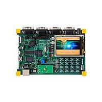
Manufacturer Part Number
IAR-KSK-IMX25
Description
KIT DEVELOPMENT I.MX257, ARM926
Manufacturer
Freescale Semiconductor
Series
i.MX25r
Type
MCUr
Datasheets
1.MCIMX25WPDKJ.pdf
(2 pages)
2.IAR-KSK-IMX25.pdf
(154 pages)
3.IAR-KSK-IMX25.pdf
(2 pages)
4.IAR-KSK-IMX25.pdf
(57 pages)
Specifications of IAR-KSK-IMX25
Contents
Board, Cables, CD, Debugger, Power Supply
Processor To Be Evaluated
I.MX257
Processor Series
i.MX25
Data Bus Width
16 bit
Interface Type
UART, JTAG, USB, Ethernet, SD/MMC
Core
ARM926EJ-S
Silicon Manufacturer
Freescale
Core Architecture
ARM
Core Sub-architecture
ARM9
Silicon Core Number
I.MX2
Silicon Family Name
I.MX25
Mcu Supported Families
I.MX25
For Use With/related Products
i.MX25
Lead Free Status / RoHS Status
Lead free / RoHS Compliant


1
2
3
4
5
6
3.7.8
Figure 54
figure. The following definitions apply to values and signals described in
84
No.
86
87
88
89
90
91
92
93
94
95
96
97
V
In the “Characteristics” column, bl = bit length, wl = word length, wr = word length relative
In the “Expression” column, T
For the internal clock, the external clock cycle is defined by Icyc and the ESAI control register.
The word-relative frame sync signal waveform relative to the clock operates in the same manner as the bit-length frame sync
signal waveform, but spreads starting from one serial clock before the first bit clock (same as the bit length frame sync signal),
until the second-to-last bit-clock of the first word in the frame.
Periodically sampled and not 100% tested.
CORE_VDD
•
•
•
SCKT rising edge to data out valid
SCKT rising edge to data out high
impedance
SCKT rising edge to transmitter #0 drive
enable negation
FST input (bl, wr) setup time before SCKT
falling edge
FST input (wl) setup time before SCKT falling
edge
FST input hold time after SCKT falling edge
FST input (wl) to data out enable from high
impedance
FST input (wl) to transmitter #0 drive enable
assertion
Flag output valid after SCKT rising edge
HCKR/HCKT clock cycle
HCKT input rising edge to SCKT output
HCKR input rising edge to SCKR output
LS: low-speed mode. Low-speed card can tolerate clocks up to 400 kHz
FS: full-speed mode. Full-speed MMC card’s clock can reach 20 MHz; full speed SD/SDIO card
clock can reach 25 MHz
HS: high-speed mode. High-speed MMC card’s clock can reach 52 MHz; SD/SDIO card clock can
reach 50 MHz
shows eSDHCv2 timing, and
Enhanced Secured Digital Host Controller (eSDHCv2) Timing
= 1.00 ± 0.10 V; T
6
5
Characteristics
i.MX25 Applications Processor for Consumer and Industrial Products, Rev. 8
6
Table 60. ESAI General Timing Requirements (continued)
C
J
= –40 °C to 125 °C, C
= 7.5 ns.
1 2
Table 61
Symbol
L
—
—
—
—
—
—
—
—
—
—
—
—
= 50 pF
describes the timing parameters (SD1–SD8) used in the
Expression
2 x T
—
—
—
—
—
—
—
—
—
—
—
C
3
Min.
18.0
18.0
2.0
2.0
4.0
5.0
15
—
—
—
—
—
—
—
—
—
—
—
—
Table
Max.
18.0
13.0
21.0
16.0
14.0
21.0
14.0
14.0
18.0
18.0
9.0
9.0
61:
—
—
—
—
—
—
—
Freescale Semiconductor
Condition
x ck
x ck
x ck
x ck
x ck
x ck
x ck
i ck
i ck
i ck
i ck
i ck
i ck
i ck
—
—
—
—
—
Unit
ns
ns
ns
ns
ns
ns
ns
ns
ns
ns
ns
ns
Related parts for IAR-KSK-IMX25
Image
Part Number
Description
Manufacturer
Datasheet
Request
R

Part Number:
Description:
Manufacturer:
Freescale Semiconductor, Inc
Datasheet:
Part Number:
Description:
Manufacturer:
Freescale Semiconductor, Inc
Datasheet:
Part Number:
Description:
Manufacturer:
Freescale Semiconductor, Inc
Datasheet:
Part Number:
Description:
Manufacturer:
Freescale Semiconductor, Inc
Datasheet:
Part Number:
Description:
Manufacturer:
Freescale Semiconductor, Inc
Datasheet:
Part Number:
Description:
Manufacturer:
Freescale Semiconductor, Inc
Datasheet:
Part Number:
Description:
Manufacturer:
Freescale Semiconductor, Inc
Datasheet:
Part Number:
Description:
Manufacturer:
Freescale Semiconductor, Inc
Datasheet:
Part Number:
Description:
Manufacturer:
Freescale Semiconductor, Inc
Datasheet:
Part Number:
Description:
Manufacturer:
Freescale Semiconductor, Inc
Datasheet:
Part Number:
Description:
Manufacturer:
Freescale Semiconductor, Inc
Datasheet:
Part Number:
Description:
Manufacturer:
Freescale Semiconductor, Inc
Datasheet:
Part Number:
Description:
Manufacturer:
Freescale Semiconductor, Inc
Datasheet:
Part Number:
Description:
Manufacturer:
Freescale Semiconductor, Inc
Datasheet:
Part Number:
Description:
Manufacturer:
Freescale Semiconductor, Inc
Datasheet: