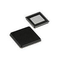
CYRF69213-40LFXC Cypress Semiconductor Corp, CYRF69213-40LFXC Datasheet - Page 19

CYRF69213-40LFXC
Manufacturer Part Number
CYRF69213-40LFXC
Description
IC PROC 8K FLASH 40VQFN
Manufacturer
Cypress Semiconductor Corp
Series
CYRFr
Type
Transceiverr
Datasheet
1.CYRF69213-40LFXC.pdf
(77 pages)
Specifications of CYRF69213-40LFXC
Package / Case
40-VQFN Exposed Pad, 40-HVQFN, 40-SQFN, 40-DHVQFN
Frequency
2.4GHz
Data Rate - Maximum
1Mbps
Modulation Or Protocol
ISM
Applications
General Purpose
Power - Output
4dBm
Sensitivity
-97dBm
Voltage - Supply
4 V ~ 5.5 V
Current - Receiving
23.4mA
Current - Transmitting
36.6mA
Data Interface
PCB, Surface Mount
Memory Size
8kB Flash, 256B SRAM
Antenna Connector
PCB, Surface Mount
Operating Temperature
0°C ~ 70°C
Operating Frequency
2497 MHz
Operating Supply Voltage
2.5 V or 3.3 V
Maximum Operating Temperature
+ 70 C
Minimum Operating Temperature
0 C
Mounting Style
SMD/SMT
Operating Temperature (min)
0C
Operating Temperature (max)
70C
Operating Temperature Classification
Commercial
Operating Supply Voltage (min)
1.8V
Operating Supply Voltage (typ)
2.5/3.3V
Operating Supply Voltage (max)
3.6V
Lead Free Status / RoHS Status
Lead free / RoHS Compliant
For Use With
770-1001 - ISP 4PORT CYPRESS ENCORE II MCU
Lead Free Status / Rohs Status
Lead free / RoHS Compliant
Other names
428-1934
Available stocks
Company
Part Number
Manufacturer
Quantity
Price
Part Number:
CYRF69213-40LFXC
Manufacturer:
CYPRESS/赛普拉斯
Quantity:
20 000
expected values, the M8C halts (with the exception of the
SWBootReset function). The following code puts the correct
value in KEY1 and KEY2. The code starts with a halt, to force the
program to jump directly into the setup code and not run into it.
halt
SSCOP: mov [KEY1], 3ah
mov X, SP
mov A, X
add A, 3
mov [KEY2], A
Table 24. SROM Function Parameters
The SROM also features Return Codes and Lockouts.
Return Codes
Return codes aid in the determination of success or failure of a
particular function. The return code is stored in KEY1’s position
in the parameter block. The CheckSum and TableRead functions
do not have return codes because KEY1’s position in the
parameter block is used to return other data.
Table 25. SROM Return Codes
Read, write, and erase operations may fail if the target block is
read or write protected. Block protection levels are set during
device programming.
The EraseAll function overwrites data in addition to leaving the
entire user Flash in the erase state. The EraseAll function loops
through the number of Flash macros in the product, executing
the following sequence: erase, bulk program all zeros, erase.
After all the user space in all the Flash macros are erased, a
second loop erases and then programs each protection block
with zeros.
Document #: 001-07552 Rev. *D
Key1/Counter/Return Code
Key2/TMP
BlockID
Pointer
Clock
Mode
Delay
PCL
Return Code
00h
01h
02h
03h
Variable Name
Success
Function not allowed due to level of protection
on block
Software reset without hardware reset
Fatal error, SROM halted
Description
SRAM Address
0,FAh
0,FBh
0,FCh
0,FDh
0,FEh
0,FFh
0,F8h
0,F9h
SROM Function Descriptions
All SROM functions are described in the following sections.
SWBootReset Function
The SROM function, SWBootReset, is the function that is
responsible for transitioning the device from a reset state to
running user code. The SWBootReset function is executed
whenever the SROM is entered with an M8C accumulator value
of 00h; the SRAM parameter block is not used as an input to the
function. This happens, by design, after a hardware reset,
because the M8C's accumulator is reset to 00h or when user
code executes the SSC instruction with an accumulator value of
00h. The SWBootReset function does not execute when the
SSC instruction is executed with a bad key value and a nonzero
function code. A CYRF69213 device executes the HALT
instruction if a bad value is given for either KEY1 or KEY2.
The SWBootReset function verifies the integrity of the calibration
data by way of a 16-bit checksum, before releasing the M8C to
run user code.
ReadBlock Function
The ReadBlock function is used to read 64 contiguous bytes
from Flash—a block.
The first thing this function does is to check the protection bits
and determine if the desired BLOCKID is readable. If read
protection is turned on, the ReadBlock function exits, setting the
accumulator and KEY2 back to 00h. KEY1 has a value of 01h,
indicating a read failure. If read protection is not enabled, the
function reads 64 bytes from the Flash using a ROMX instruction
and store the results in SRAM using an MVI instruction. The first
of the 64 bytes is stored in SRAM at the address indicated by the
value of the POINTER parameter. When the ReadBlock
completes successfully, the accumulator, KEY1, and KEY2 all
have a value of 00h.
Table 26. ReadBlock Parameters
WriteBlock Function
The WriteBlock function is used to store data in the Flash. Data
is moved 64 bytes at a time from SRAM to Flash using this
function. The first thing the WriteBlock function does is to check
the protection bits and determine if the desired BLOCKID is
writable. If write protection is turned on, the WriteBlock function
exits, setting the accumulator and KEY2 back to 00h. KEY1 has
a value of 01h, indicating a write failure. The configuration of the
WriteBlock function is straightforward. The BLOCKID of the
Flash block, where the data is stored, must be determined and
stored at SRAM address FAh.
KEY1
KEY2
BLOCKID
POINTER
Name
0,F8h
0,F9h
0,FAh
0,FBh
Address
3Ah
Stack Pointer value, when SSC is
executed
Flash block number
First of 64 addresses in SRAM
where returned data should be
stored
Description
CYRF69213
Page 19 of 77
[+] Feedback


