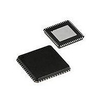
CYRF69213-40LFXC Cypress Semiconductor Corp, CYRF69213-40LFXC Datasheet - Page 9

CYRF69213-40LFXC
Manufacturer Part Number
CYRF69213-40LFXC
Description
IC PROC 8K FLASH 40VQFN
Manufacturer
Cypress Semiconductor Corp
Series
CYRFr
Type
Transceiverr
Datasheet
1.CYRF69213-40LFXC.pdf
(77 pages)
Specifications of CYRF69213-40LFXC
Package / Case
40-VQFN Exposed Pad, 40-HVQFN, 40-SQFN, 40-DHVQFN
Frequency
2.4GHz
Data Rate - Maximum
1Mbps
Modulation Or Protocol
ISM
Applications
General Purpose
Power - Output
4dBm
Sensitivity
-97dBm
Voltage - Supply
4 V ~ 5.5 V
Current - Receiving
23.4mA
Current - Transmitting
36.6mA
Data Interface
PCB, Surface Mount
Memory Size
8kB Flash, 256B SRAM
Antenna Connector
PCB, Surface Mount
Operating Temperature
0°C ~ 70°C
Operating Frequency
2497 MHz
Operating Supply Voltage
2.5 V or 3.3 V
Maximum Operating Temperature
+ 70 C
Minimum Operating Temperature
0 C
Mounting Style
SMD/SMT
Operating Temperature (min)
0C
Operating Temperature (max)
70C
Operating Temperature Classification
Commercial
Operating Supply Voltage (min)
1.8V
Operating Supply Voltage (typ)
2.5/3.3V
Operating Supply Voltage (max)
3.6V
Lead Free Status / RoHS Status
Lead free / RoHS Compliant
For Use With
770-1001 - ISP 4PORT CYPRESS ENCORE II MCU
Lead Free Status / Rohs Status
Lead free / RoHS Compliant
Other names
428-1934
Available stocks
Company
Part Number
Manufacturer
Quantity
Price
Part Number:
CYRF69213-40LFXC
Manufacturer:
CYPRESS/赛普拉斯
Quantity:
20 000
taken and may be read through the SPI interface. An RSSI
reading is taken automatically when the start of a packet is
detected. In addition, a new RSSI reading is taken every time the
previous reading is read from the RSSI register, allowing the
background RF energy level on any given channel to be easily
measured when RSSI is read when no signal is being received.
A new reading can occur as fast as once every 12 μ s.
SPI Interface
The SPI interface between the MCU function and the radio
function is a 3-wire SPI Interface. The three pins are MOSI
(Master Out Slave In), SCK (Serial Clock), SS (Slave Select).
There is an alternate 4-wire MISO Interface that requires the
connection of two external pins. The SPI interface is controlled
by configuring the SPI Configure Register (SICR Address:
0x3D).
3-Wire SPI Interface
The radio function receives a clock from the MCU function on the
SCK pin. The MOSI pin is multiplexed with the MISO pin. Bidirec-
tional data transfer takes place between the MCU function and
the radio function through this multiplexed MOSI pin. When using
this mode the user firmware should ensure that the MOSI pin on
the MCU function is in a high impedance state, except when the
MCU is actively transmitting data. Firmware must also control the
direction of data flow and switch directions between MCU
function and radio function by setting the SWAP bit [Bit 7] of the
SPI Configure Register. The SS pin is asserted prior to initiating
a data transfer between the MCU function and the radio function.
The IRQ function may be optionally multiplexed with the MOSI
pin; when this option is enabled the IRQ function is not available
while the SS pin is low. When using this configuration, user
firmware should ensure that the MOSI function on MCU function
is in a high impedance state whenever SS is high.
Figure 4. 3-Wire SPI Mode
4-Wire SPI Interface
The 4-wire SPI communications interface consists of MOSI,
MISO, SCK, and SS.
The device receives SCK from the MCU function on the SCK pin.
Data from the MCU function is shifted in on the MOSI pin. Data
Document #: 001-07552 Rev. *D
MCU Function
P1.5/MOSI
P1.4/SCK
P1.3/nSS
MOSI/MISO multiplexed
on one MOSI pin
SCK
MOSI
nSS
Radio Function
to the MCU function is shifted out on the MISO pin. The active
low SS pin must be asserted for the two functions to commu-
nicate. The IRQ function may be optionally multiplexed with the
MOSI pin; when this option is enabled the IRQ function is not
available while the SS pin is low. When using this configuration,
user firmware should ensure that the MOSI function on MCU
function is in a high impedance state whenever SS is high.
Figure 5. 4-WIRE SPI Mode
SPI Communication and Transactions
The SPI transactions can be single byte or multi-byte. The MCU
function initiates a data transfer through a Command/Address
byte. The following bytes are data bytes. The SPI transaction
format is shown in
The DIR bit specifies the direction of data transfer. 0 = Master
reads from slave. 1 = Master writes to slave.
The INC bit helps to read or write consecutive bytes from
contiguous memory locations in a single burst mode operation.
If Slave Select is asserted and INC = 1, then the master MCU
function reads a byte from the radio, the address is incremented
by a byte location, and then the byte at that location is read, and
so on. If Slave Select is asserted and INC = 0, then the MCU
function reads/writes the bytes in the same register in burst
mode, but if it is a register file then it reads/writes the bytes in
that register file.
The SPI interface between the radio function and the MCU is not
dependent on the internal 12 MHz oscillator of the radio.
Therefore, radio function registers can be read from or written
into while the radio is in sleep mode.
SPI I/O Voltage References
The SPI interfaces between MCU function and the radio and the
IRQ and RST have a separate voltage reference V
the radio function to directly interface with the MCU function,
which operates at higher supply voltage. The internal SPIO pins
between the MCU function and radio function should be
connected with a regulated voltage of 3.3V (by setting [bit4] of
Registers P13CR, P14CR, P15CR, and P16CR of the MCU
function) and the internal 3.3V regulator of the MCU function
should be turned on.
P1.6/MISO
MCU Function
P1.5/MOSI
This connection is external to the PRoC LP Chip
P1.4/SCK
P1.3/nSS
Figure
6.
nSS
MOSI
SCK
Radio Function
CYRF69213
Page 9 of 77
IO
MISO
, enabling
[+] Feedback


