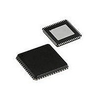
CYRF69213-40LFXC Cypress Semiconductor Corp, CYRF69213-40LFXC Datasheet - Page 43

CYRF69213-40LFXC
Manufacturer Part Number
CYRF69213-40LFXC
Description
IC PROC 8K FLASH 40VQFN
Manufacturer
Cypress Semiconductor Corp
Series
CYRFr
Type
Transceiverr
Datasheet
1.CYRF69213-40LFXC.pdf
(77 pages)
Specifications of CYRF69213-40LFXC
Package / Case
40-VQFN Exposed Pad, 40-HVQFN, 40-SQFN, 40-DHVQFN
Frequency
2.4GHz
Data Rate - Maximum
1Mbps
Modulation Or Protocol
ISM
Applications
General Purpose
Power - Output
4dBm
Sensitivity
-97dBm
Voltage - Supply
4 V ~ 5.5 V
Current - Receiving
23.4mA
Current - Transmitting
36.6mA
Data Interface
PCB, Surface Mount
Memory Size
8kB Flash, 256B SRAM
Antenna Connector
PCB, Surface Mount
Operating Temperature
0°C ~ 70°C
Operating Frequency
2497 MHz
Operating Supply Voltage
2.5 V or 3.3 V
Maximum Operating Temperature
+ 70 C
Minimum Operating Temperature
0 C
Mounting Style
SMD/SMT
Operating Temperature (min)
0C
Operating Temperature (max)
70C
Operating Temperature Classification
Commercial
Operating Supply Voltage (min)
1.8V
Operating Supply Voltage (typ)
2.5/3.3V
Operating Supply Voltage (max)
3.6V
Lead Free Status / RoHS Status
Lead free / RoHS Compliant
For Use With
770-1001 - ISP 4PORT CYPRESS ENCORE II MCU
Lead Free Status / Rohs Status
Lead free / RoHS Compliant
Other names
428-1934
Available stocks
Company
Part Number
Manufacturer
Quantity
Price
Part Number:
CYRF69213-40LFXC
Manufacturer:
CYPRESS/赛普拉斯
Quantity:
20 000
Serial Peripheral Interface (SPI)
The SPI Master/Slave Interface core logic runs on the SPI clock domain, making its functionality independent of system clock speed.
SPI is a four pin serial interface comprised of a clock, an enable and two data pins.
Document #: 001-07552 Rev. *D
Slave Select Output Enable
Master Out, Slave In, OE
Master IN, Slave Out OE
SPI State Machine
Register Block
Sclk Output Enable
Master/Slave Sel
Little Endian Sel
SCK Speed Sel
SCK Polarity
SCK Phase
Data (8 bit)
Data (8 bit)
Empty
SS_N
Load
Load
Full
LE_SEL
LE_SEL
SS_N_OE
MISO_OE
MOSI_OE
SCK_OE
SCK
Figure 15. SPI Block Diagram
SCK Clock Phase/Polarity
SCK Clock Generation
Output Shift Buffer
SCK Clock Select
Input Shift Buffer
Shift Buffer
Select
Master/Slave Set
SCK
GPIO Block
MISO/MOSI
Crossbar
SS_N
SCK_OE
SS_N_OE
MISO_OE
MOSI_OE
CYRF69213
Page 43 of 77
MISO
MOSI
SCK
SS_N
[+] Feedback


