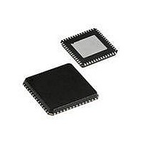
CYRF69213-40LFXC Cypress Semiconductor Corp, CYRF69213-40LFXC Datasheet - Page 36

CYRF69213-40LFXC
Manufacturer Part Number
CYRF69213-40LFXC
Description
IC PROC 8K FLASH 40VQFN
Manufacturer
Cypress Semiconductor Corp
Series
CYRFr
Type
Transceiverr
Datasheet
1.CYRF69213-40LFXC.pdf
(77 pages)
Specifications of CYRF69213-40LFXC
Package / Case
40-VQFN Exposed Pad, 40-HVQFN, 40-SQFN, 40-DHVQFN
Frequency
2.4GHz
Data Rate - Maximum
1Mbps
Modulation Or Protocol
ISM
Applications
General Purpose
Power - Output
4dBm
Sensitivity
-97dBm
Voltage - Supply
4 V ~ 5.5 V
Current - Receiving
23.4mA
Current - Transmitting
36.6mA
Data Interface
PCB, Surface Mount
Memory Size
8kB Flash, 256B SRAM
Antenna Connector
PCB, Surface Mount
Operating Temperature
0°C ~ 70°C
Operating Frequency
2497 MHz
Operating Supply Voltage
2.5 V or 3.3 V
Maximum Operating Temperature
+ 70 C
Minimum Operating Temperature
0 C
Mounting Style
SMD/SMT
Operating Temperature (min)
0C
Operating Temperature (max)
70C
Operating Temperature Classification
Commercial
Operating Supply Voltage (min)
1.8V
Operating Supply Voltage (typ)
2.5/3.3V
Operating Supply Voltage (max)
3.6V
Lead Free Status / RoHS Status
Lead free / RoHS Compliant
For Use With
770-1001 - ISP 4PORT CYPRESS ENCORE II MCU
Lead Free Status / Rohs Status
Lead free / RoHS Compliant
Other names
428-1934
Available stocks
Company
Part Number
Manufacturer
Quantity
Price
Part Number:
CYRF69213-40LFXC
Manufacturer:
CYPRESS/赛普拉斯
Quantity:
20 000
ECO Trim Register
Table 45. ECO (ECO_TR) [0x1EB] [R/W]
General-Purpose I/O Ports
The general purpose I/O ports are discussed in the following sections.
Port Data Registers
Table 46. P0 Data Register (P0DATA)[0x00] [R/W]
Document #: 001-07552 Rev. *D
Bit #
Field
Read/Write
Default
This register controls the ratios (in numbers of 32 kHz clock periods) of ‘on’ time versus ‘off’ time for LVD and POR detection circuit
Bits 7:6
Bit #
Field
Read/Write
Default
This register contains the data for Port 0. Writing to this register sets the bit values to be output on output enabled pins. Reading
from this register returns the current state of the Port 0 pins
Bit 7
Bits 6:5
Bits 4:3
Bit 2
Bit 1
Bit 0
Sleep Duty Cycle [1:0]
0 0 = 1/128 periods of the Internal 32 kHz Low speed Oscillator
0 1 = 1/512 periods of the Internal 32 kHz Low speed Oscillator
1 0 = 1/32 periods of the Internal 32 kHz Low speed Oscillator
1 1 = 1/8 periods of the Internal 32 kHz Low speed Oscillato
P0.7 Data
Reserved
The use of the pins as the P0.6–P0.5 GPIOs and the alternative functions exist in the CYRF69213
P0.4–P0.3 Data/INT2 – INT1
In addition to their use as the P0.4–P0.3 GPIOs, these pins can also be used for the alternative functions as the Inter-
rupt pins (INT0–INT2). To configure the P0.4–P0.3 pins, refer to the P0.3/INT1–P0.4/INT2 Configuration Register
(Table
The use of the pins as the P0.4–P0.3 GPIOs and the alternative functions exist in the CYRF69213
Reserved
P0.1
Reserved
Sleep Duty Cycle [1:0]
R/W
P0.7
R/W
50)
7
0
7
0
Reserved
R/W
R/W
6
0
6
0
Reserved
R/W
5
–
0
5
0
P0.4/INT2
R/W
4
–
0
4
0
r
P0.3/INT1
R/W
3
–
0
3
0
Reserved
Reserved
R/W
2
–
0
2
0
P0.1
R/W
1
–
0
1
0
CYRF69213
Page 36 of 77
Reserved
R/W
0
–
0
0
0
[+] Feedback


