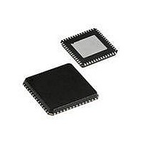
CYRF69213-40LFXC Cypress Semiconductor Corp, CYRF69213-40LFXC Datasheet - Page 57

CYRF69213-40LFXC
Manufacturer Part Number
CYRF69213-40LFXC
Description
IC PROC 8K FLASH 40VQFN
Manufacturer
Cypress Semiconductor Corp
Series
CYRFr
Type
Transceiverr
Datasheet
1.CYRF69213-40LFXC.pdf
(77 pages)
Specifications of CYRF69213-40LFXC
Package / Case
40-VQFN Exposed Pad, 40-HVQFN, 40-SQFN, 40-DHVQFN
Frequency
2.4GHz
Data Rate - Maximum
1Mbps
Modulation Or Protocol
ISM
Applications
General Purpose
Power - Output
4dBm
Sensitivity
-97dBm
Voltage - Supply
4 V ~ 5.5 V
Current - Receiving
23.4mA
Current - Transmitting
36.6mA
Data Interface
PCB, Surface Mount
Memory Size
8kB Flash, 256B SRAM
Antenna Connector
PCB, Surface Mount
Operating Temperature
0°C ~ 70°C
Operating Frequency
2497 MHz
Operating Supply Voltage
2.5 V or 3.3 V
Maximum Operating Temperature
+ 70 C
Minimum Operating Temperature
0 C
Mounting Style
SMD/SMT
Operating Temperature (min)
0C
Operating Temperature (max)
70C
Operating Temperature Classification
Commercial
Operating Supply Voltage (min)
1.8V
Operating Supply Voltage (typ)
2.5/3.3V
Operating Supply Voltage (max)
3.6V
Lead Free Status / RoHS Status
Lead free / RoHS Compliant
For Use With
770-1001 - ISP 4PORT CYPRESS ENCORE II MCU
Lead Free Status / Rohs Status
Lead free / RoHS Compliant
Other names
428-1934
Available stocks
Company
Part Number
Manufacturer
Quantity
Price
Part Number:
CYRF69213-40LFXC
Manufacturer:
CYPRESS/赛普拉斯
Quantity:
20 000
Endpoint 0 Mode
Because both firmware and the SIE are allowed to write to the
Endpoint 0 Mode and Count Registers the SIE provides an inter-
locking mechanism to prevent accidental overwriting of data.
Table 82. Endpoint 0 Mode (EP0MODE) [0x44] [R/W]
Document #: 001-07552 Rev. *D
Bit #
Field
Read/Write
Default
Bit 7
Bit 6
Bit 5
Bit 4
Bits 3:0
SETUP Received
This bit is set by hardware when a valid SETUP packet is received. It is forced HIGH from the start of the data
packet phase of the SETUP transactions until the end of the data phase of a control write transfer and cannot be
cleared during this interval. While this bit is set to ‘1’, the CPU cannot write to the EP0 FIFO. This prevents firm-
ware from overwriting an incoming SETUP transaction before firmware has a chance to read the SETUP data
This bit is cleared by any non-locked writes to the register
0 = No SETUP received
1 = SETUP received
IN Received
This bit, when set, indicates a valid IN packet has been received. This bit is updated to ‘1’ after the host acknowl-
edges an IN data packet.When clear, it indicates that either no IN has been received or that the host didn’t
acknowledge the IN data by sending an ACK handshake
This bit is cleared by any non-locked writes to the register.
0 = No IN received
1 = IN received
OUT Received
This bit, when set, indicates a valid OUT packet has been received and ACKed. This bit is updated to ‘1’ after the
last received packet in an OUT transaction. When clear, it indicates no OUT received
This bit is cleared by any non-locked writes to the register
0 = No OUT received
1 = OUT received
ACK’d Transaction
The ACK’d transaction bit is set whenever the SIE engages in a transaction to the register’s endpoint that com-
pletes with a ACK packet
This bit is cleared by any non-locked writes to the register
1 = The transaction completes with an ACK
0 = The transaction does not complete with an ACK
Mode [3:0]
The endpoint modes determine how the SIE responds to USB traffic that the host sends to the endpoint. The
mode controls how the USB SIE responds to traffic and how the USB SIE changes the mode of that endpoint as a
result of host packets to the endpoint
Received
R/C[3]
Setup
7
0
IN Received
R/C[3]
6
0
OUT Re-
ceived
R/C[3]
5
0
ACK’d Trans
R/C[3]
4
0
When the SIE writes to these registers they are locked and the
processor cannot write to them until after it has read them.
Writing to this register clears the upper four bits regardless of the
value written.
R/W
3
0
R/W
2
0
Mode[3:0]
R/W
1
0
CYRF69213
Page 57 of 77
R/W
0
0
[+] Feedback


