CYRF69213-40LFXC Cypress Semiconductor Corp, CYRF69213-40LFXC Datasheet - Page 4
CYRF69213-40LFXC
Manufacturer Part Number
CYRF69213-40LFXC
Description
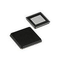
IC PROC 8K FLASH 40VQFN
Manufacturer
Cypress Semiconductor Corp
Series
CYRFr
Type
Transceiverr
Datasheet
1.CYRF69213-40LFXC.pdf
(77 pages)
Specifications of CYRF69213-40LFXC
Package / Case
40-VQFN Exposed Pad, 40-HVQFN, 40-SQFN, 40-DHVQFN
Frequency
2.4GHz
Data Rate - Maximum
1Mbps
Modulation Or Protocol
ISM
Applications
General Purpose
Power - Output
4dBm
Sensitivity
-97dBm
Voltage - Supply
4 V ~ 5.5 V
Current - Receiving
23.4mA
Current - Transmitting
36.6mA
Data Interface
PCB, Surface Mount
Memory Size
8kB Flash, 256B SRAM
Antenna Connector
PCB, Surface Mount
Operating Temperature
0°C ~ 70°C
Operating Frequency
2497 MHz
Operating Supply Voltage
2.5 V or 3.3 V
Maximum Operating Temperature
+ 70 C
Minimum Operating Temperature
0 C
Mounting Style
SMD/SMT
Operating Temperature (min)
0C
Operating Temperature (max)
70C
Operating Temperature Classification
Commercial
Operating Supply Voltage (min)
1.8V
Operating Supply Voltage (typ)
2.5/3.3V
Operating Supply Voltage (max)
3.6V
Lead Free Status / RoHS Status
Lead free / RoHS Compliant
For Use With
770-1001 - ISP 4PORT CYPRESS ENCORE II MCU
Lead Free Status / Rohs Status
Lead free / RoHS Compliant
Other names
428-1934
Available stocks
Company
Part Number
Manufacturer
Quantity
Price

Part Number:
CYRF69213-40LFXC
Manufacturer:
CYPRESS/赛普拉斯
Quantity:
20 000


Pin Configuration
PRoC LP Functional Overview
The SoC is designed to implement wireless device links
operating in the worldwide 2.4 GHz ISM frequency band. It is
intended for systems compliant with worldwide regulations
covered by ETSI EN 301 489-1 V1.41, ETSI EN 300 328-1
V1.3.1 (Europe), FCC CFR 47 Part 15 (USA and Industry
Canada) and TELEC ARIB_T66_March, 2003 (Japan).
The SoC contains a 2.4 GHz 1 Mbps GFSK radio transceiver,
packet data buffering, packet framer, DSSS baseband controller,
Received Signal Strength Indication (RSSI), and SPI interface
for data transfer and device configuration.
The radio supports 98 discrete 1 MHz channels (regulations may
limit the use of some of these channels in certain jurisdictions).
In
spreading/despreading, while in GFSK Mode (1 Mb/s - GFSK)
the baseband performs Start of Frame (SOF), End of Frame
(EOF) detection and CRC16 generation and checking. The
baseband may also be configured to automatically transmit
Acknowledge (ACK) handshake packets whenever a valid
packet is received.
Document #: 001-07552 Rev. *D
DSSS
Pin
29
30
31
32
33
34
35
36
37
38
40
41
42
modes
Corner Tabs
V
PACTL
XOUT
Name
Reset
E-pad
MISO
the
P1.6
P1.7
DD_1.8
P0.7
V
V
L/D
(continued)
reg
IO
baseband
Master In Slave Out, from radio function. Can be configured as GPIO
Bufferd CLK, PACTL_n or GPIO
Control for external PA or GPIO
GPIO. Port 1 Bit 6
I/O interface voltage. Connected to pin 24 via 0.047 μ F
Radio Reset. Connected to V
a RESET = HIGH event the very first time power is applied to the radio otherwise the state of
the radio function control registers is unknown
GPIO. Port 1 Bit 7
Regulated logic bypass. Connected via 0.47 μ F to GND
Connected to GND
GPIO. Port 0 Bit 7
Connected to pin 24
Must be connected to GND
Do not connect corner tabs
performs
DSSS
DD
When in receive mode, with packet framing enabled, the device
is always ready to receive data transmitted at any of the
supported bit rates, except SDR, enabling the implementation of
mixed-rate systems in which different devices use different data
rates. This also enables the implementation of dynamic data rate
systems, which use high data rates at shorter distances and/or
in a low moderate interference environment, and change to lower
data rates at longer distances and/or in high interference
environments.
The MCU function is an 8-bit Flash programmable microcon-
troller with integrated low speed USB interface. The instruction
set has been optimized specifically for USB operations, although
it can be used for a variety of other embedded applications.
The MCU function has up to eight Kbytes of Flash for user’s code
and up to 256 bytes of RAM for stack space and user variables.
In addition, the MCU function includes a Watchdog timer, a
vectored interrupt controller, a 16-bit Free-Running Timer, and
12-bit Programmable Interrupt Timer.
The MCU function supports in-system programming by using the
D+ and D– pins as the serial programming mode interface. The
programming protocol is not USB.
via 0.47 μ F capacitor or to microcontroller GPIO pin. Must have
Function
CYRF69213
Page 4 of 77
[+] Feedback
Related parts for CYRF69213-40LFXC
Image
Part Number
Description
Manufacturer
Datasheet
Request
R

Part Number:
Description:
Manufacturer:
Cypress Semiconductor Corp
Datasheet:
Part Number:
Description:
Manufacturer:
Cypress Semiconductor Corp
Datasheet:
Part Number:
Description:
Manufacturer:
Cypress Semiconductor Corp
Datasheet:
Part Number:
Description:
Manufacturer:
Cypress Semiconductor Corp
Datasheet:
Part Number:
Description:
Manufacturer:
Cypress Semiconductor Corp
Datasheet: