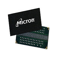
MT47H32M16HR-3:F Micron Technology Inc, MT47H32M16HR-3:F Datasheet - Page 103

MT47H32M16HR-3:F
Manufacturer Part Number
MT47H32M16HR-3:F
Description
IC DDR2 SDRAM 512MBIT 3NS 84FBGA
Manufacturer
Micron Technology Inc
Type
DDR2 SDRAMr
Datasheet
1.MT47H32M16HR-3F.pdf
(132 pages)
Specifications of MT47H32M16HR-3:F
Format - Memory
RAM
Memory Type
DDR2 SDRAM
Memory Size
512M (32Mx16)
Speed
3ns
Interface
Parallel
Voltage - Supply
1.7 V ~ 1.9 V
Operating Temperature
0°C ~ 85°C
Package / Case
84-TFBGA
Organization
32Mx16
Density
512Mb
Address Bus
15b
Access Time (max)
450ps
Maximum Clock Rate
667MHz
Operating Supply Voltage (typ)
1.8V
Package Type
FBGA
Operating Temp Range
0C to 85C
Operating Supply Voltage (max)
1.9V
Operating Supply Voltage (min)
1.7V
Supply Current
250mA
Pin Count
84
Mounting
Surface Mount
Operating Temperature Classification
Commercial
Lead Free Status / RoHS Status
Lead free / RoHS Compliant
Other names
557-1466
Available stocks
Company
Part Number
Manufacturer
Quantity
Price
Company:
Part Number:
MT47H32M16HR-3:F
Manufacturer:
Micron Technology Inc
Quantity:
10 000
Part Number:
MT47H32M16HR-3:F
Manufacturer:
MICRON/美光
Quantity:
20 000
Company:
Part Number:
MT47H32M16HR-3:F(D9JLR)
Manufacturer:
TOSH
Quantity:
1 225
Company:
Part Number:
MT47H32M16HR-3:F(D9JLR)
Manufacturer:
MICRON
Quantity:
1 000
Part Number:
MT47H32M16HR-3:FTR
Manufacturer:
MICRON/镁光
Quantity:
20 000
Table 43: WRITE Using Concurrent Auto Precharge
PDF: 09005aef82f1e6e2
512MbDDR2.pdf - Rev. R 12/10 EN
WRITE with auto precharge
From Command
(Bank n)
the WRITE diagrams show the nominal case, and where the two extreme cases (
[MIN] and
(page 104) shows the nominal case and the extremes of
tion of a burst, assuming no other commands have been initiated, the DQ will remain
High-Z and any additional input data will be ignored.
Data for any WRITE burst may be concatenated with a subsequent WRITE command to
provide continuous flow of input data. The first data element from the new burst is ap-
plied after the last element of a completed burst. The new WRITE command should be
issued x cycles after the first WRITE command, where x equals BL/2.
Figure 57 (page 105) shows concatenated bursts of BL = 4 and how full-speed random
write accesses within a page or pages can be performed. An example of nonconsecutive
WRITEs is shown in Figure 58 (page 105). DDR2 SDRAM supports concurrent auto pre-
charge options, as shown in Table 43.
DDR2 SDRAM does not allow interrupting or truncating any WRITE burst using BL = 4
operation. Once the BL = 4 WRITE command is registered, it must be allowed to com-
plete the entire WRITE burst cycle. However, a WRITE BL = 8 operation (with auto
precharge disabled) might be interrupted and truncated only by another WRITE burst
as long as the interruption occurs on a 4-bit boundary due to the 4n-prefetch architec-
ture of DDR2 SDRAM. WRITE burst BL = 8 operations may not be interrupted or
truncated with any command except another WRITE command, as shown in Figure 59
(page 106).
Data for any WRITE burst may be followed by a subsequent READ command. To follow
a WRITE,
cycles required to meet
WRITE burst may be followed by a subsequent PRECHARGE command.
met, as shown in Figure 61 (page 108).
less of the data mask condition.
WRITE or WRITE with auto precharge
READ or READ with auto precharge
t
PRECHARGE or ACTIVATE
WTR should be met, as shown in Figure 60 (page 107). The number of clock
t
DQSS [MAX]) might not be intuitive, they have also been included. Figure 56
To Command
(Bank m)
t
WTR is either 2 or
103
t
Micron Technology, Inc. reserves the right to change products or specifications without notice.
WR starts at the end of the data burst, regard-
t
512Mb: x4, x8, x16 DDR2 SDRAM
WTR/
(with Concurrent Auto Precharge)
t
CK, whichever is greater. Data for any
(CL - 1) + (BL/2) +
Minimum Delay
t
DQSS for BL = 4. Upon comple-
(BL/2)
1
© 2004 Micron Technology, Inc. All rights reserved.
t
WTR
t
WR must be
WRITE
t
DQSS
Units
t
t
t
CK
CK
CK


