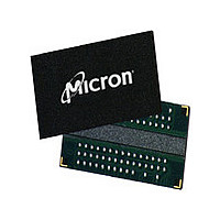
MT47H32M16HR-3:F Micron Technology Inc, MT47H32M16HR-3:F Datasheet - Page 76

MT47H32M16HR-3:F
Manufacturer Part Number
MT47H32M16HR-3:F
Description
IC DDR2 SDRAM 512MBIT 3NS 84FBGA
Manufacturer
Micron Technology Inc
Type
DDR2 SDRAMr
Datasheet
1.MT47H32M16HR-3F.pdf
(132 pages)
Specifications of MT47H32M16HR-3:F
Format - Memory
RAM
Memory Type
DDR2 SDRAM
Memory Size
512M (32Mx16)
Speed
3ns
Interface
Parallel
Voltage - Supply
1.7 V ~ 1.9 V
Operating Temperature
0°C ~ 85°C
Package / Case
84-TFBGA
Organization
32Mx16
Density
512Mb
Address Bus
15b
Access Time (max)
450ps
Maximum Clock Rate
667MHz
Operating Supply Voltage (typ)
1.8V
Package Type
FBGA
Operating Temp Range
0C to 85C
Operating Supply Voltage (max)
1.9V
Operating Supply Voltage (min)
1.7V
Supply Current
250mA
Pin Count
84
Mounting
Surface Mount
Operating Temperature Classification
Commercial
Lead Free Status / RoHS Status
Lead free / RoHS Compliant
Other names
557-1466
Available stocks
Company
Part Number
Manufacturer
Quantity
Price
Company:
Part Number:
MT47H32M16HR-3:F
Manufacturer:
Micron Technology Inc
Quantity:
10 000
Part Number:
MT47H32M16HR-3:F
Manufacturer:
MICRON/美光
Quantity:
20 000
Company:
Part Number:
MT47H32M16HR-3:F(D9JLR)
Manufacturer:
TOSH
Quantity:
1 225
Company:
Part Number:
MT47H32M16HR-3:F(D9JLR)
Manufacturer:
MICRON
Quantity:
1 000
Part Number:
MT47H32M16HR-3:FTR
Manufacturer:
MICRON/镁光
Quantity:
20 000
Burst Length
Figure 34: MR Definition
PDF: 09005aef82f1e6e2
512MbDDR2.pdf - Rev. R 12/10 EN
Notes:
Burst length is defined by bits M0–M2, as shown in Figure 34. Read and write accesses
to the DDR2 SDRAM are burst-oriented, with the burst length being programmable to
either four or eight. The burst length determines the maximum number of column loca-
tions that can be accessed for a given READ or WRITE command.
When a READ or WRITE command is issued, a block of columns equal to the burst
length is effectively selected. All accesses for that burst take place within this block,
meaning that the burst will wrap within the block if a boundary is reached. The block is
uniquely selected by A2–Ai when BL = 4 and by A3–Ai when BL = 8 (where Ai is the most
significant column address bit for a given configuration). The remaining (least signifi-
cant) address bit(s) is (are) used to select the starting location within the block. The
programmed burst length applies to both read and write bursts.
0
BA2
16
M15
1. M16 (BA2) is only applicable for densities ≥1Gb, reserved for future use, and must be
2. Mode bits (Mn) with corresponding address balls (An) greater than M12 (A12) are re-
3. Not all listed WR and CL options are supported in any individual speed grade.
1
0
0
1
1
BA1
15
MR
M14
programmed to “0.”
served for future use and must be programmed to “0.”
14
BA0
M12
0
1
0
1
0
1
0
M11
n
An
Extended mode register (EMR2)
Extended mode register (EMR3)
0
0
0
0
1
1
1
1
Extended mode register (EMR)
(low power)
PD Mode
Slow exit
2
(normal)
PD
Fast exit
Mode Register Definition
12
M10
A12 A11
0
0
1
1
0
0
1
1
Mode register (MR)
11
M9
0
1
0
1
0
1
0
1
WR
10
A10
Write Recovery
9
Reserved
A9
M8
DLL TM
0
1
2
3
4
5
6
7
8
8
A8
M7
DLL Reset
0
1
7
A7 A6 A5 A4 A3
Yes
No
CAS#
Normal
Mode
6
Test
Latency
5
M6
76
0
0
0
0
1
1
1
1
4
M5
BT
0
0
1
1
0
0
1
1
3
M3
0
1
M4
Burst Length
M2
0
1
0
1
0
1
0
1
0
0
0
0
1
1
1
1
2
A2 A1 A0
M1
0
0
1
1
0
0
1
1
1
M0
Micron Technology, Inc. reserves the right to change products or specifications without notice.
0
1
0
1
0
1
0
1
CAS Latency (CL)
Burst Type
Interleaved
Sequential
0
Burst Length
Reserved
Reserved
Reserved
Reserved
Reserved
Reserved
Reserved
Reserved
Reserved
512Mb: x4, x8, x16 DDR2 SDRAM
3
4
5
6
7
Address Bus
Mode Register (Mx)
4
8
Mode Register (MR)
© 2004 Micron Technology, Inc. All rights reserved.


