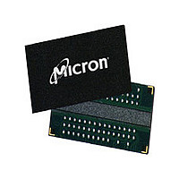
MT47H32M16HR-3:F Micron Technology Inc, MT47H32M16HR-3:F Datasheet - Page 125

MT47H32M16HR-3:F
Manufacturer Part Number
MT47H32M16HR-3:F
Description
IC DDR2 SDRAM 512MBIT 3NS 84FBGA
Manufacturer
Micron Technology Inc
Type
DDR2 SDRAMr
Datasheet
1.MT47H32M16HR-3F.pdf
(132 pages)
Specifications of MT47H32M16HR-3:F
Format - Memory
RAM
Memory Type
DDR2 SDRAM
Memory Size
512M (32Mx16)
Speed
3ns
Interface
Parallel
Voltage - Supply
1.7 V ~ 1.9 V
Operating Temperature
0°C ~ 85°C
Package / Case
84-TFBGA
Organization
32Mx16
Density
512Mb
Address Bus
15b
Access Time (max)
450ps
Maximum Clock Rate
667MHz
Operating Supply Voltage (typ)
1.8V
Package Type
FBGA
Operating Temp Range
0C to 85C
Operating Supply Voltage (max)
1.9V
Operating Supply Voltage (min)
1.7V
Supply Current
250mA
Pin Count
84
Mounting
Surface Mount
Operating Temperature Classification
Commercial
Lead Free Status / RoHS Status
Lead free / RoHS Compliant
Other names
557-1466
Available stocks
Company
Part Number
Manufacturer
Quantity
Price
Company:
Part Number:
MT47H32M16HR-3:F
Manufacturer:
Micron Technology Inc
Quantity:
10 000
Part Number:
MT47H32M16HR-3:F
Manufacturer:
MICRON/美光
Quantity:
20 000
Company:
Part Number:
MT47H32M16HR-3:F(D9JLR)
Manufacturer:
TOSH
Quantity:
1 225
Company:
Part Number:
MT47H32M16HR-3:F(D9JLR)
Manufacturer:
MICRON
Quantity:
1 000
Part Number:
MT47H32M16HR-3:FTR
Manufacturer:
MICRON/镁光
Quantity:
20 000
Figure 78: RESET Function
PDF: 09005aef82f1e6e2
512MbDDR2.pdf - Rev. R 12/10 EN
Bank address
Command
Address
ODT
DQS 3
DM 3
CK#
CKE
A10
DQ 3
R
CK
TT
Bank a
READ
Col n
T0
High-Z
High-Z
Notes:
NOP 2
T1
1. V
2. Either NOP or DESELECT command may be applied.
3. DM represents DM for x4/x8 configuration and UDM, LDM for x16 configuration. DQS
4. In certain cases where a READ cycle is interrupted, CKE going HIGH may result in the
5. Initialization timing is shown in Figure 41 (page 86).
represents DQS, DQS#, UDQS, UDQS#, LDQS, LDQS#, RDQS, and RDQS# for the appropri-
ate configuration (x4, x8, x16).
completion of the burst.
DD
Bank b
Col n
READ
, V
T2
DDL
, V
DDQ
NOP 2
Indicates a break in
time scale
T3
, V
DO
TT
, and V
DO
NOP 2
T4
125
System
DO
RESET
REF
must be valid at all times.
t DELAY
Unknown
T5
Micron Technology, Inc. reserves the right to change products or specifications without notice.
512Mb: x4, x8, x16 DDR2 SDRAM
1
R
TT
On
High-Z
High-Z
Transitioning Data
t CL
© 2004 Micron Technology, Inc. All rights reserved.
t CK
Start of normal 5
initialization
t CL
sequence
NOP 2
Ta0
4
T = 400ns (MIN)
t CKE (MIN)
All banks
Tb0
PRE
Don’t Care
High-Z
t RPA
Reset


