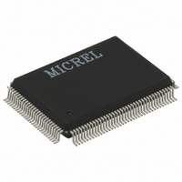
KSZ8893FQL-FX Micrel Inc, KSZ8893FQL-FX Datasheet - Page 18

KSZ8893FQL-FX
Manufacturer Part Number
KSZ8893FQL-FX
Description
2+1 Port 10/100 Switch W/Tranceivers & Frame Buffers, ( )
Manufacturer
Micrel Inc
Datasheet
1.KSZ8893FQL-FX.pdf
(117 pages)
Specifications of KSZ8893FQL-FX
Controller Type
Ethernet Switch Controller
Interface
MII, RMII, SNI
Voltage - Supply
3.1 V ~ 3.5 V
Operating Temperature
-40°C ~ 85°C
Mounting Type
Surface Mount
Package / Case
128-MQFP, 128-PQFP
Number Of Primary Switch Ports
3
Internal Memory Buffer Size
32
Operating Supply Voltage (typ)
3.3V
Fiber Support
Yes
Integrated Led Drivers
Yes
Power Supply Type
Analog/Digital
Package Type
PQFP
Vlan Support
Yes
Operating Temperature (max)
70C
Operating Temperature (min)
0C
Pin Count
128
Mounting
Surface Mount
Jtag Support
No
Operating Temperature Classification
Commercial
Data Rate
1000Mbps
Lead Free Status / RoHS Status
Lead free / RoHS Compliant
For Use With
576-1603 - EVAL KIT EXPERIMENTAL KSZ8893MQL
Current - Supply
-
Lead Free Status / RoHS Status
Compliant, Lead free / RoHS Compliant
Other names
576-3273
Available stocks
Company
Part Number
Manufacturer
Quantity
Price
Company:
Part Number:
KSZ8893FQL-FX
Manufacturer:
Micrel Inc
Quantity:
1 950
Company:
Part Number:
KSZ8893FQL-FX
Manufacturer:
FSC
Quantity:
1 800
Micrel, Inc.
October 2007
Number
Pin
65
66
67
68
69
70
71
72
73
74
75
76
77
78
79
80
81
82
83
84
85
86
Pin Name
LEDSEL0
SMRXDV
UNUSED
UNUSED
SMTXEN
SMTXER
SMRXD3
SMRXD2
SMRXD1
SMRXD0
SMTXD3
SMTXD2
SMTXD1
SMTXD0
SMTXC /
REFCLK
SMRXC
RST_N
VDDIO
DGND
SCOL
X1
X2
Type
Ipd/O
Ipd/O
Ipd/O
Gnd
Ipu
I/O
I/O
I/O
I/O
O
O
P
I
I
I
I
I
I
I
I
I
I
(1)
Pin Function
25MHz crystal/oscillator clock connections
Pins (X1, X2) connect to a crystal. If an oscillator is used, X1 connects to a 3.3V
tolerant oscillator and X2 is no connected.
Note: Clock is ±50ppm for both crystal and oscillator.
Unused pin – externally pull down for normal operation
Unused pin – externally pull down for normal operation
LED display mode select
See description in pins 1 and 4.
Switch MII transmit clock (MII and SNI modes only)
Reference Clock (RMII mode only)
Note: In RMII mode, pin X1 is pulled up to VDDIO supply with a 10K resistor and pin
X2 is a no connect.
Digital ground
3.3V digital V
Switch MII receive clock.
Switch MII receive data bit 3
Strap option: switch MII full-duplex flow control
Switch MII receive data bit 2
Strap option: switch MII is in
Switch MII receive data bit 1
Strap option: Switch MII is in
Switch MII receive data bit 0
Strap option: switch will accept packet size up to
Hardware Reset (active low)
Switch MII transmit enable
Switch MII transmit data bit 3
Switch MII transmit data bit 2
Switch MII transmit data bit 1
Switch MII transmit data bit 0
Switch MII transmit error
Switch MII receive data valid
Switch MII collision detect
Output in PHY MII mode
Input in MAC MII mode
PD (default) = disable
PU = enable
PD (default) = full-duplex mode
PU = half-duplex mode
PD (default) = 100Mbps mode
PU = 10Mbps mode
PD = 1536 bytes (inclusive)
PU = 1522 bytes (tagged), 1518 bytes (untagged)
Output in PHY MII mode and SNI mode
Input in MAC MII mode
Input for 50MHz ±50ppm system clock
DD
18
M9999-101607-1.3
KSZ8893FQL


