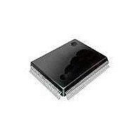
SAA7115HLBE NXP Semiconductors, SAA7115HLBE Datasheet - Page 122

SAA7115HLBE
Manufacturer Part Number
SAA7115HLBE
Description
Video ICs ADV DGTL VIDEO DECODR
Manufacturer
NXP Semiconductors
Datasheet
1.SAA7115HLBE.pdf
(548 pages)
Specifications of SAA7115HLBE
Operating Supply Voltage
3.3 V
Maximum Operating Temperature
+ 70 C
Package / Case
SOT-407
Minimum Operating Temperature
0 C
Mounting Style
SMD/SMT
Number Of Channels
2
Resolution
8 bit
Lead Free Status / RoHS Status
Lead free / RoHS Compliant
Other names
SAA7115HL/V1,557 SAF7115HLBE
- Current page: 122 of 548
- Download datasheet (6Mb)
PNX1300/01/02/11 Data Book
Figure 7-25. YUV 4:2:0 to YUV 4:2:2 co-sited conversion.
automatically by mirroring the first and last pixels of each
line. For example:
• Output pixel 1 uses input pixel 1 to generate its
Figure 7-26. 2x upscaling of Y pixels.
Figure 7-27. 2x upscaling of U and V with interspersed to co-sited conversion.
7-12
Output Pixels: YU’V’ 4:2:2
value. (same location, no filtering).
Input Pixels: YUV 4:2:0
Output Pixels: Y’U’V’
Output Pixels: Y’U’V’
Input Pixels: YUV
Input Pixels: YUV
Y0,0
PRELIMINARY SPECIFICATION
U0,0; V0,0
Y0,0; U0,0; V0,0
Upscaled Luminance Output Between
Input Pixels: Y’ = (-3,19,19,-3)/32 × Y
Co-sited Chrominance Output
U’,V’ = (–1,5,13,–1)/16×U,V
Co-sited Chrominance Output:
U’,V’ = (–1,5,13,–1)/16×U,V
Output Location Same
As Input Pixel: Y’U’V’ = YUV
Chrominance (U,V)
samples
Chrominance (U,V)
samples
Chrominance (U,V)
samples
• Output pixel 2 uses pixels 1,1, 2 and 3 to generate its
• Output pixel 3 uses pixel 2 to generate its value.
• Output pixel 4 pixel uses pixels 1, 2, 3 and 4, etc.
value.
Luminance
Co-sited Chrominance Output
U’,V’ = (–1,13,5,–1)/16×U,V
samples
Luminance
Upscaled Luminance Output Between
Luminance
Input Pixels: Y’ = (-3,19,19,-3)/32×Y
samples
samples
Upscaled Luminance Output Same
As Input Pixel: Y’ = Y
Upscaled Chrominance Output Between
Input Pixels: U’,V’ = (-3,19,19,-3)/32 × U,V
Philips Semiconductors
Y0
Y1
Y2
Y3
Y0, U0, V0
Y1, U0, V0
Y2, U2, V2
Y3, U2, V2
U0, V0
U2, V2
Related parts for SAA7115HLBE
Image
Part Number
Description
Manufacturer
Datasheet
Request
R
Part Number:
Description:
Ntsc/pal/secam 9-bit Video Decoder
Manufacturer:
NXP Semiconductors
Datasheet:
Part Number:
Description:
NXP Semiconductors designed the LPC2420/2460 microcontroller around a 16-bit/32-bitARM7TDMI-S CPU core with real-time debug interfaces that include both JTAG andembedded trace
Manufacturer:
NXP Semiconductors
Datasheet:

Part Number:
Description:
NXP Semiconductors designed the LPC2458 microcontroller around a 16-bit/32-bitARM7TDMI-S CPU core with real-time debug interfaces that include both JTAG andembedded trace
Manufacturer:
NXP Semiconductors
Datasheet:
Part Number:
Description:
NXP Semiconductors designed the LPC2468 microcontroller around a 16-bit/32-bitARM7TDMI-S CPU core with real-time debug interfaces that include both JTAG andembedded trace
Manufacturer:
NXP Semiconductors
Datasheet:
Part Number:
Description:
NXP Semiconductors designed the LPC2470 microcontroller, powered by theARM7TDMI-S core, to be a highly integrated microcontroller for a wide range ofapplications that require advanced communications and high quality graphic displays
Manufacturer:
NXP Semiconductors
Datasheet:
Part Number:
Description:
NXP Semiconductors designed the LPC2478 microcontroller, powered by theARM7TDMI-S core, to be a highly integrated microcontroller for a wide range ofapplications that require advanced communications and high quality graphic displays
Manufacturer:
NXP Semiconductors
Datasheet:
Part Number:
Description:
The Philips Semiconductors XA (eXtended Architecture) family of 16-bit single-chip microcontrollers is powerful enough to easily handle the requirements of high performance embedded applications, yet inexpensive enough to compete in the market for hi
Manufacturer:
NXP Semiconductors
Datasheet:
Part Number:
Description:
The XA-S3 device is a member of Philips Semiconductors? XA(eXtended Architecture) family of high performance 16-bitsingle-chip microcontrollers
Manufacturer:
NXP Semiconductors
Datasheet:

Part Number:
Description:
The NXP BlueStreak LH75401/LH75411 family consists of two low-cost 16/32-bit System-on-Chip (SoC) devices
Manufacturer:
NXP Semiconductors
Datasheet:

Part Number:
Description:
The NXP LPC3130/3131 combine an 180 MHz ARM926EJ-S CPU core, high-speed USB2
Manufacturer:
NXP Semiconductors
Datasheet:

Part Number:
Description:
The NXP LPC3141 combine a 270 MHz ARM926EJ-S CPU core, High-speed USB 2
Manufacturer:
NXP Semiconductors

Part Number:
Description:
The NXP LPC3143 combine a 270 MHz ARM926EJ-S CPU core, High-speed USB 2
Manufacturer:
NXP Semiconductors

Part Number:
Description:
The NXP LPC3152 combines an 180 MHz ARM926EJ-S CPU core, High-speed USB 2
Manufacturer:
NXP Semiconductors

Part Number:
Description:
The NXP LPC3154 combines an 180 MHz ARM926EJ-S CPU core, High-speed USB 2
Manufacturer:
NXP Semiconductors


