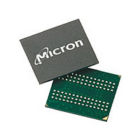
MT46H8M32LFB5-6 IT:H Micron Technology Inc, MT46H8M32LFB5-6 IT:H Datasheet - Page 26

MT46H8M32LFB5-6 IT:H
Manufacturer Part Number
MT46H8M32LFB5-6 IT:H
Description
DRAM Chip DDR SDRAM 256M-Bit 8Mx32 1.8V 90-Pin VFBGA Tray
Manufacturer
Micron Technology Inc
Type
DDR SDRAMr
Datasheet
1.MT46H8M32LFB5-6_ITH.pdf
(96 pages)
Specifications of MT46H8M32LFB5-6 IT:H
Density
256 Mb
Maximum Clock Rate
166 MHz
Package
90VFBGA
Address Bus Width
14 Bit
Operating Supply Voltage
1.8 V
Maximum Random Access Time
6.5|5 ns
Operating Temperature
-40 to 85 °C
Organization
8Mx32
Address Bus
14b
Access Time (max)
6.5/5ns
Operating Supply Voltage (typ)
1.8V
Package Type
VFBGA
Operating Temp Range
-40C to 85C
Operating Supply Voltage (max)
1.95V
Operating Supply Voltage (min)
1.7V
Supply Current
120mA
Pin Count
90
Mounting
Surface Mount
Operating Temperature Classification
Industrial
Lead Free Status / RoHS Status
Compliant
Table 9: Electrical Characteristics and Recommended AC Operating Conditions (Continued)
Notes 1–9 apply to all parameters in this table; V
PDF: 09005aef834bf85b
256mb_mobile_ddr_sdram_t36n.pdf - Rev. H 11/09 EN
Parameter
DQS read
preamble
DQS read postamble
Active bank a to active bank
b command
Read of SRR to next valid
command
SRR to read
DQS write preamble
DQS write preamble setup
time
DQS write postamble
Write recovery time
Internal WRITE-to-READ
command delay
Exit power-down mode to
first valid command
Exit self refresh to first valid
command
CL = 2
Notes:
Symbol
t
1. All voltages referenced to V
2. All parameters assume proper device initialization.
3. Tests for AC timing and electrical AC and DC characteristics may be conducted at nomi-
4. The circuit shown below represents the timing reference load used in defining the rele-
5. The CK/CK# input reference voltage level (for timing referenced to CK/CK#) is the point
t
WPRES
t
t
t
WPRE
t
WPST
t
RPRE
t
t
t
RPST
t
WTR
RRD
t
SRC
SRR
XSR
WR
XP
nal supply voltage levels, but the related specifications and device operation are guaran-
teed for the full voltage ranges specified.
vant timing parameters of the device. It is not intended to be either a precise representa-
tion of the typical system environment or a depiction of the actual load presented by a
production tester. System designers will use IBIS or other simulation tools to correlate
the timing reference load to system environment. Specifications are correlated to produc-
tion test conditions (generally a coaxial transmission line terminated at the tester elec-
tronics). For the half-strength driver with a nominal 10pF load, parameters
are expected to be in the same range. However, these parameters are not subject to
production test but are estimated by design/characterization. Use of IBIS or other simula-
tion tools for system design validation is suggested.
at which CK and CK# cross; the input reference voltage level for signals other than CK/
CK# is V
I/O
Full drive strength
CL + 1
Min
0.25
DDQ
0.5
0.4
0.4
10
15
80
2
0
1
1
50
/2.
-5
Electrical Specifications – AC Operating Conditions
DD
Max
/V
1.1
0.6
0.6
–
–
–
–
–
–
–
–
–
DDQ
20pF
= 1.70–1.95V
CL + 1
Min
10.8
0.25
0.5
0.4
0.4
15
80
26
2
0
1
1
SS
-54
.
I/O
256Mb: x16, x32 Mobile LPDDR SDRAM
Max
1.1
0.6
0.6
Half drive strength
–
–
–
–
–
–
–
–
–
Micron Technology, Inc. reserves the right to change products or specifications without notice.
50
CL + 1
Min
0.25
0.5
0.4
0.4
12
15
80
2
0
1
1
-6
Max
1.1
0.6
0.6
10pF
–
–
–
–
–
–
–
–
–
CL + 1
Min
0.25
0.5
0.4
0.4
15
15
80
2
0
1
1
©2008 Micron Technology, Inc. All rights reserved.
-75
Max
1.1
0.6
0.6
–
–
–
–
–
–
–
–
–
Unit
t
t
t
t
t
t
t
t
t
ns
ns
ns
ns
CK
CK
CK
CK
CK
CK
CK
CK
AC and
Notes
24, 25
26
27
28
t
QH


