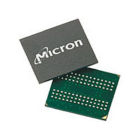
MT46H8M32LFB5-6 IT:H Micron Technology Inc, MT46H8M32LFB5-6 IT:H Datasheet - Page 74

MT46H8M32LFB5-6 IT:H
Manufacturer Part Number
MT46H8M32LFB5-6 IT:H
Description
DRAM Chip DDR SDRAM 256M-Bit 8Mx32 1.8V 90-Pin VFBGA Tray
Manufacturer
Micron Technology Inc
Type
DDR SDRAMr
Datasheet
1.MT46H8M32LFB5-6_ITH.pdf
(96 pages)
Specifications of MT46H8M32LFB5-6 IT:H
Density
256 Mb
Maximum Clock Rate
166 MHz
Package
90VFBGA
Address Bus Width
14 Bit
Operating Supply Voltage
1.8 V
Maximum Random Access Time
6.5|5 ns
Operating Temperature
-40 to 85 °C
Organization
8Mx32
Address Bus
14b
Access Time (max)
6.5/5ns
Operating Supply Voltage (typ)
1.8V
Package Type
VFBGA
Operating Temp Range
-40C to 85C
Operating Supply Voltage (max)
1.95V
Operating Supply Voltage (min)
1.7V
Supply Current
120mA
Pin Count
90
Mounting
Surface Mount
Operating Temperature Classification
Industrial
Lead Free Status / RoHS Status
Compliant
- Current page: 74 of 96
- Download datasheet (4Mb)
Figure 37: Random WRITE Cycles
PDF: 09005aef834bf85b
256mb_mobile_ddr_sdram_t36n.pdf - Rev. H 11/09 EN
Command
Address
DQ
DQS
CK#
DM
CK
3,4
Notes:
WRITE
Bank,
Col b
T0
1,2
1. Each WRITE command can be to any bank.
2. Programmed BL = 2, 4, 8, or 16 in cases shown.
3. D
4. b' (or x, n, a, g) = the next data-in following D
t
DQSS (NOM)
med burst order.
IN
b (or x, n, a, g) = data-in for column b (or x, n, q, g).
WRITE
Bank,
Col x
D
T1
IN
1,2
T1n
D
IN
WRITE
Bank,
Col n
T2
D
IN
1,2
74
T2n
D
IN
256Mb: x16, x32 Mobile LPDDR SDRAM
WRITE
Micron Technology, Inc. reserves the right to change products or specifications without notice.
Bank,
Col a
T3
D
IN
1,2
T3n
D
Don’t Care
IN
IN
b (x, n, a, g) according to the program-
WRITE
Bank,
Col g
T4
D
IN
1,2
T4n
D
IN
Transitioning Data
©2008 Micron Technology, Inc. All rights reserved.
WRITE Operation
NOP
D
T5
IN
T5n
D
IN
Related parts for MT46H8M32LFB5-6 IT:H
Image
Part Number
Description
Manufacturer
Datasheet
Request
R

Part Number:
Description:
IC SDRAM 64MBIT 133MHZ 54TSOP
Manufacturer:
Micron Technology Inc
Datasheet:

Part Number:
Description:
IC SDRAM 64MBIT 5.5NS 86TSOP
Manufacturer:
Micron Technology Inc
Datasheet:

Part Number:
Description:
IC SDRAM 64MBIT 200MHZ 86TSOP
Manufacturer:
Micron Technology Inc
Datasheet:

Part Number:
Description:
IC SDRAM 64MBIT 133MHZ 54TSOP
Manufacturer:
Micron Technology Inc
Datasheet:

Part Number:
Description:
IC SDRAM 128MBIT 133MHZ 54TSOP
Manufacturer:
Micron Technology Inc
Datasheet:

Part Number:
Description:
IC SDRAM 256MBIT 133MHZ 90VFBGA
Manufacturer:
Micron Technology Inc
Datasheet:

Part Number:
Description:
IC SDRAM 128MBIT 133MHZ 54TSOP
Manufacturer:
Micron Technology Inc
Datasheet:

Part Number:
Description:
IC SDRAM 256MBIT 133MHZ 54TSOP
Manufacturer:
Micron Technology Inc
Datasheet:

Part Number:
Description:
IC DDR SDRAM 512MBIT 6NS 66TSOP
Manufacturer:
Micron Technology Inc
Datasheet:

Part Number:
Description:
IC SDRAM 128MBIT 167MHZ 86TSOP
Manufacturer:
Micron Technology Inc
Datasheet:

Part Number:
Description:
IC SDRAM 128MBIT 143MHZ 86TSOP
Manufacturer:
Micron Technology Inc
Datasheet:

Part Number:
Description:
SDRAM 256M-BIT 1.8V 54-PIN VFBGA
Manufacturer:
Micron Technology Inc
Datasheet:

Part Number:
Description:
IC SDRAM 128MBIT 143MHZ 86TSOP
Manufacturer:
Micron Technology Inc
Datasheet:

Part Number:
Description:
IC SDRAM 128MBIT 125MHZ 54VFBGA
Manufacturer:
Micron Technology Inc
Datasheet:

Part Number:
Description:
IC SDRAM 128MBIT 125MHZ 54VFBGA
Manufacturer:
Micron Technology Inc
Datasheet:


