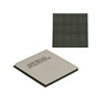
EP4SGX530HH35C2N Altera, EP4SGX530HH35C2N Datasheet - Page 74

EP4SGX530HH35C2N
Manufacturer Part Number
EP4SGX530HH35C2N
Description
IC STRATIX IV FPGA 530K 1152HBGA
Manufacturer
Altera
Series
Stratix® IV GXr
Datasheets
1.EP4SGX110DF29C3N.pdf
(80 pages)
2.EP4SGX110DF29C3N.pdf
(1154 pages)
3.EP4SGX110DF29C3N.pdf
(432 pages)
4.EP4SGX110DF29C3N.pdf
(22 pages)
5.EP4SGX110DF29C3N.pdf
(30 pages)
6.EP4SGX110DF29C3N.pdf
(72 pages)
7.EP4SGX530HH35C2N.pdf
(1145 pages)
Specifications of EP4SGX530HH35C2N
Number Of Logic Elements/cells
531200
Number Of Labs/clbs
21248
Total Ram Bits
27376
Number Of I /o
564
Voltage - Supply
0.87 V ~ 0.93 V
Mounting Type
Surface Mount
Operating Temperature
0°C ~ 85°C
Package / Case
1152-HBGA
Family Name
Stratix® IV
Number Of Logic Blocks/elements
531200
# Registers
424960
# I/os (max)
560
Process Technology
40nm
Operating Supply Voltage (typ)
900mV
Logic Cells
531200
Ram Bits
28033024
Operating Supply Voltage (min)
0.87V
Operating Supply Voltage (max)
0.93V
Operating Temp Range
0C to 85C
Operating Temperature Classification
Commercial
Mounting
Surface Mount
Pin Count
1152
Package Type
FCHBGA
Lead Free Status / RoHS Status
Lead free / RoHS Compliant
Number Of Gates
-
Lead Free Status / Rohs Status
Compliant
Available stocks
Company
Part Number
Manufacturer
Quantity
Price
1–66
Table 1–53. Glossary Table (Part 4 of 4)
Document Revision History
Table 1–54. Document Revision History (Part 1 of 3)
Stratix IV Device Handbook Volume 4: Device Datasheet and Addendum
April 2011
March 2011
March 2011
February 2011
February 2011
X, Y, Z
Letter
W
V
Date
V
V
V
V
V
V
V
V
V
V
V
V
V
V
V
V
W
CM(DC)
ICM
ID
DIF(AC)
DIF(DC)
IH
IH(AC)
IH(DC)
IL
IL(AC)
IL(DC)
OCM
OD
SWING
X
OX
Subject
—
Version
Table 1–54
5.0
4.9
4.8
4.7
4.6
DC Common mode input voltage.
Input Common mode voltage—The common mode of the differential signal at the receiver.
Input differential voltage swing—The difference in voltage between the positive and
complementary conductors of a differential transmission at the receiver.
AC differential input voltage—Minimum AC input differential voltage required for switching.
DC differential input voltage— Minimum DC input differential voltage required for switching.
Voltage input high—The minimum positive voltage applied to the input which is accepted by
the device as a logic high.
High-level AC input voltage
High-level DC input voltage
Voltage input low—The maximum positive voltage applied to the input which is accepted by
the device as a logic low.
Low-level AC input voltage
Low-level DC input voltage
Output Common mode voltage—The common mode of the differential signal at the
transmitter.
Output differential voltage swing—The difference in voltage between the positive and
complementary conductors of a differential transmission at the transmitter.
Differential input voltage
Input differential cross point voltage
Output differential cross point voltage
High-speed I/O block: Clock Boost Factor
■
■
■
■
■
■
■
■
Updated
Table
Updated Table 1–24.
Removed (Note 17) in Table 1-24.
Added (Note 17) to Table 1–24.
Updated Table 1–1, Table 1–5, Table 1–23, Table 1–24, Table 1–30, Table 1–31, Table
1–32, Table 1–34, Table 1–37, Table 1–41, and Table 1–51.
Updated the “Recommended Operating Conditions” section.
Added the “Schmitt Trigger Input” section.April
Minor text edits.
lists the revision history for this chapter.
1–24.
Table
1–1,
Table
1–5,
Table
Chapter 1: DC and Switching Characteristics for Stratix IV Devices
1–6,
Definitions
Changes
—
Table
1–13,
Table
1–16,
April 2011 Altera Corporation
Table
Document Revision History
1–23, and


