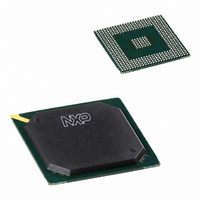
PNX1500E/G,557 NXP Semiconductors, PNX1500E/G,557 Datasheet - Page 104

PNX1500E/G,557
Manufacturer Part Number
PNX1500E/G,557
Description
IC MEDIA PROC 240MHZ 456-BGA
Manufacturer
NXP Semiconductors
Specifications of PNX1500E/G,557
Applications
Multimedia
Core Processor
TriMedia
Controller Series
Nexperia
Interface
I²C, 2-Wire Serial
Number Of I /o
61
Voltage - Supply
1.14 V ~ 1.26 V
Operating Temperature
0°C ~ 85°C
Mounting Type
Surface Mount
Package / Case
456-BGA
Lead Free Status / RoHS Status
Lead free / RoHS Compliant
Program Memory Type
-
Ram Size
-
Lead Free Status / Rohs Status
Compliant
Other names
568-1296
935277746557
PNX1500E/G
935277746557
PNX1500E/G
- Current page: 104 of 828
- Download datasheet (4Mb)
NXP Semiconductors
Volume 1 of 1
PNX15XX_PNX952X_SER_N_4
Product data sheet
10.3.2 Simple Peripheral Capabilities (‘XIO-8/16’)
PNX15xx/952x Series as PCI master allows TM3260 to generate all single cycle PCI
transaction types, including memory cycles, I/O cycles, configuration cycles and
interrupt acknowledge cycles. As PCI target, PNX15xx/952x Series responds to
memory transactions and configuration type cycles, but not to I/O cycles.
PNX15xx/952x Series can act as PCI bus arbiter for up to 3 external masters, i.e.
total of 4 masters with PNX15xx/952x Series, without external logic.
PCI clock is an input to PNX15xx/952x Series, but if desired the general purpose
PNX15xx/952x Series PCI_SYS_CLK clock output can be used as the PCI 33 MHz
clock for the entire system.
Table 8
Table 8: PNX15xx/952x Series PCI capabilities
The 16-bit micro-processor peripheral interface is a master-only interface, and
provides non-multiplexed address and data lines. A total of 26 address bits are
provided, as well as a bi-directional, 16-bit data bus. Five device profiles are provided,
each generating a chip-select for external devices. Up to 64 MB of address space is
allowed per device profile. The interface control signals are compatible with a
Motorola 68360 bus interface, and support both fixed wait-state or dynamic
completion acknowledgment.
A total of 5 pre-decoded Chip Select pins are available to accommodate typical
outside slave configurations with minimal or no external glue logic. Each chip select
pin has an associated programmable address range within the XIO address space.
Each chip select pin can also choose to obey external DTACK completion signalling,
or be set to have a pre-programmed number of wait cycles.
The peripheral interface derives 24 of the 26 address wires and 8 out of the 16 data
wires from the PCI AD[31:0] pins. The remaining pins are XIO specific and non PCI
shared. An ‘XIO’ access looks like a valid PCI transaction to PCI master/targets on
the same wires. Unused XIO pins are available as GPIO pins.
As PCI Target it responds to
Memory Read
Memory Write
Configuration Read
Configuration Write
Memory Read Multiple
Memory Read Line
Memory Write and Invalidate
summarizes the PCI features supported by the PNX15xx/952x Series.
Rev. 4.0 — 03 December 2007
As PCI master it initiates
IO Read
IO Write
Memory Read
Memory Write
Configuration Read
Configuration Write
Memory Read Multiple
Memory Read Line
Memory Write and Invalidate
Interrupt Acknowledge
PNX15xx/952x Series
Chapter 2: Overview
© NXP B.V. 2007. All rights reserved.
2-104
Related parts for PNX1500E/G,557
Image
Part Number
Description
Manufacturer
Datasheet
Request
R

Part Number:
Description:
Manufacturer:
NXP Semiconductors
Datasheet:
Part Number:
Description:
Digital Signal Processors & Controllers - DSP, DSC NEXPERIA MEDIA PROC 240MHZ
Manufacturer:
NXP Semiconductors
Part Number:
Description:
Digital Signal Processors & Controllers - DSP, DSC PNX1500, 240MHZ
Manufacturer:
NXP Semiconductors
Part Number:
Description:
NXP Semiconductors designed the LPC2420/2460 microcontroller around a 16-bit/32-bitARM7TDMI-S CPU core with real-time debug interfaces that include both JTAG andembedded trace
Manufacturer:
NXP Semiconductors
Datasheet:

Part Number:
Description:
NXP Semiconductors designed the LPC2458 microcontroller around a 16-bit/32-bitARM7TDMI-S CPU core with real-time debug interfaces that include both JTAG andembedded trace
Manufacturer:
NXP Semiconductors
Datasheet:
Part Number:
Description:
NXP Semiconductors designed the LPC2468 microcontroller around a 16-bit/32-bitARM7TDMI-S CPU core with real-time debug interfaces that include both JTAG andembedded trace
Manufacturer:
NXP Semiconductors
Datasheet:
Part Number:
Description:
NXP Semiconductors designed the LPC2470 microcontroller, powered by theARM7TDMI-S core, to be a highly integrated microcontroller for a wide range ofapplications that require advanced communications and high quality graphic displays
Manufacturer:
NXP Semiconductors
Datasheet:
Part Number:
Description:
NXP Semiconductors designed the LPC2478 microcontroller, powered by theARM7TDMI-S core, to be a highly integrated microcontroller for a wide range ofapplications that require advanced communications and high quality graphic displays
Manufacturer:
NXP Semiconductors
Datasheet:
Part Number:
Description:
The Philips Semiconductors XA (eXtended Architecture) family of 16-bit single-chip microcontrollers is powerful enough to easily handle the requirements of high performance embedded applications, yet inexpensive enough to compete in the market for hi
Manufacturer:
NXP Semiconductors
Datasheet:
Part Number:
Description:
The XA-S3 device is a member of Philips Semiconductors? XA(eXtended Architecture) family of high performance 16-bitsingle-chip microcontrollers
Manufacturer:
NXP Semiconductors
Datasheet:

Part Number:
Description:
The NXP BlueStreak LH75401/LH75411 family consists of two low-cost 16/32-bit System-on-Chip (SoC) devices
Manufacturer:
NXP Semiconductors
Datasheet:

Part Number:
Description:
The NXP LPC3130/3131 combine an 180 MHz ARM926EJ-S CPU core, high-speed USB2
Manufacturer:
NXP Semiconductors
Datasheet:

Part Number:
Description:
The NXP LPC3141 combine a 270 MHz ARM926EJ-S CPU core, High-speed USB 2
Manufacturer:
NXP Semiconductors

Part Number:
Description:
The NXP LPC3143 combine a 270 MHz ARM926EJ-S CPU core, High-speed USB 2
Manufacturer:
NXP Semiconductors


