MPC8343VRAGDB Freescale Semiconductor, MPC8343VRAGDB Datasheet - Page 15
MPC8343VRAGDB
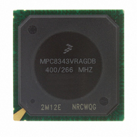
Manufacturer Part Number
MPC8343VRAGDB
Description
IC MPU POWERQUICC II 620-PBGA
Manufacturer
Freescale Semiconductor
Series
PowerQUICC II PROr
Datasheet
1.MPC8343VRAGDB.pdf
(79 pages)
Specifications of MPC8343VRAGDB
Processor Type
MPC83xx PowerQUICC II Pro 32-Bit
Speed
400MHz
Voltage
1.2V
Mounting Type
Surface Mount
Package / Case
620-PBGA
Processor Series
MPC8xxx
Core
e300
Data Bus Width
32 bit
Development Tools By Supplier
MPC8349E-MITXE
Maximum Clock Frequency
400 MHz
Maximum Operating Temperature
+ 105 C
Mounting Style
SMD/SMT
I/o Voltage
1.8 V, 2.5 V, 3.3 V
Minimum Operating Temperature
0 C
Core Size
32 Bit
Program Memory Size
64KB
Cpu Speed
400MHz
Embedded Interface Type
I2C, SPI, USB, UART
Digital Ic Case Style
BGA
No. Of Pins
620
Rohs Compliant
Yes
Family Name
MPC83xx
Device Core
PowerQUICC II Pro
Device Core Size
32b
Frequency (max)
400MHz
Instruction Set Architecture
RISC
Supply Voltage 1 (typ)
1.2V
Operating Supply Voltage (max)
1.26V
Operating Supply Voltage (min)
1.14V
Operating Temp Range
0C to 105C
Operating Temperature Classification
Commercial
Mounting
Surface Mount
Pin Count
620
Package Type
BGA
For Use With
CWH-PPC-8343N-VX - KIT EVAL SYSTEM QUICCSTART 8248CWH-PPC-8343N-VE - EVALUATION SYSTEM QUICC MPC8343E
Lead Free Status / RoHS Status
Lead free / RoHS Compliant
Features
-
Lead Free Status / Rohs Status
Lead free / RoHS Compliant
Available stocks
Company
Part Number
Manufacturer
Quantity
Price
Company:

Part Number:
MPC8343VRAGDB
Manufacturer:
Freescale Semiconductor
Quantity:
135
Company:
Part Number:
MPC8343VRAGDB
Manufacturer:
Freescale Semiconductor
Quantity:
10 000
Part Number:
MPC8343VRAGDB
Manufacturer:
FREESCALE
Quantity:
20 000


Table 13
Table 14
GV
Freescale Semiconductor
I/O reference voltage
I/O termination voltage
Input high voltage
Input low voltage
Output leakage current
Output high current (V
Output low current (V
Notes:
1. GV
2. MV
3. V
4. Output leakage is measured with all outputs disabled, 0 V
Input/output capacitance: DQ, DQS, DQS
Delta input/output capacitance: DQ, DQS, DQS
Note:
1. This parameter is sampled. GV
I/O supply voltage
I/O reference voltage
I/O termination voltage
Input high voltage
Input low voltage
Output leakage current
Output high current (V
on MV
MV
DD
TT
DD
REF
REF
is not applied directly to the device. It is the supply to which far end signal termination is made and is expected to equal
(typ) = 2.5 V
is expected to be within 50 mV of the DRAM GV
REF
. This rail should track variations in the DC level of MV
is expected to equal 0.5 × GV
provides the DDR2 capacitance when GV
provides the recommended operating conditions for the DDR SDRAM component(s) when
Table 12. DDR2 SDRAM DC Electrical Characteristics for GV
Parameter/Condition
MPC8343EA PowerQUICC II Pro Integrated Host Processor Hardware Specifications, Rev. 10
cannot exceed ±2% of the DC value.
Parameter/Condition
Table 14. DDR SDRAM DC Electrical Characteristics for GV
OUT
OUT
OUT
.
= 0.280 V)
= 1.420 V)
= 1.95 V)
Table 13. DDR2 SDRAM Capacitance for GV
DD
= 1.8 V ± 0.090 V, f = 1 MHz, T
DD
, and to track GV
Symbol
MV
MV
GV
V
I
V
V
I
V
I
V
I
V
I
OZ
OH
OH
OL
OZ
TT
TT
REF
IH
IH
IL
REF
IL
DD
DD
DD
at all times.
≤
DD
DC variations as measured at the receiver. Peak-to-peak noise
V
MV
REF
MV
Symbol
0.49 × GV
(typ) =
OUT
MV
MV
0.49 × GV
C
REF
C
.
REF
DIO
–13.4
A
IO
REF
REF
–0.3
–9.9
13.4
≤
2.375
–15.2
–0.3
–9.9
= 25°C, V
Min
+ 0.125
GV
– 0.04
1.8 V.
+ 0.18
– 0.04
DD
DD
DD
.
OUT
DD
Min
—
6
DD
(typ) = 1.8 V
= GV
MV
MV
(typ) = 1.8 V (continued)
0.51 × GV
MV
MV
GV
0.51 × GV
GV
REF
REF
DD
DD
DD
REF
REF
2.625
9.9
DD
—
—
Max
–9.9
/2, V
—
– 0.125
(typ) = 2.5 V
+ 0.04
+ 0.3
+ 0.04
+ 0.3
– 0.18
Max
0.5
DD
OUT
8
DD
(peak-to-peak) = 0.2 V.
DDR and DDR2 SDRAM
Unit
Unit
mA
mA
mA
μA
μA
pF
pF
V
V
V
V
V
V
V
V
V
Notes
Notes
—
—
—
—
—
—
—
2
3
4
1
2
3
4
1
1
15
Related parts for MPC8343VRAGDB
Image
Part Number
Description
Manufacturer
Datasheet
Request
R

Part Number:
Description:
Manufacturer:
Freescale Semiconductor, Inc
Datasheet:
Part Number:
Description:
Manufacturer:
Freescale Semiconductor, Inc
Datasheet:
Part Number:
Description:
Manufacturer:
Freescale Semiconductor, Inc
Datasheet:
Part Number:
Description:
Manufacturer:
Freescale Semiconductor, Inc
Datasheet:
Part Number:
Description:
Manufacturer:
Freescale Semiconductor, Inc
Datasheet:
Part Number:
Description:
Manufacturer:
Freescale Semiconductor, Inc
Datasheet:
Part Number:
Description:
Manufacturer:
Freescale Semiconductor, Inc
Datasheet:
Part Number:
Description:
Manufacturer:
Freescale Semiconductor, Inc
Datasheet:
Part Number:
Description:
Manufacturer:
Freescale Semiconductor, Inc
Datasheet:
Part Number:
Description:
Manufacturer:
Freescale Semiconductor, Inc
Datasheet:
Part Number:
Description:
Manufacturer:
Freescale Semiconductor, Inc
Datasheet:
Part Number:
Description:
Manufacturer:
Freescale Semiconductor, Inc
Datasheet:
Part Number:
Description:
Manufacturer:
Freescale Semiconductor, Inc
Datasheet:
Part Number:
Description:
Manufacturer:
Freescale Semiconductor, Inc
Datasheet:
Part Number:
Description:
Manufacturer:
Freescale Semiconductor, Inc
Datasheet: