MPC8343VRAGDB Freescale Semiconductor, MPC8343VRAGDB Datasheet - Page 60
MPC8343VRAGDB
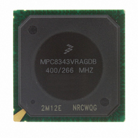
Manufacturer Part Number
MPC8343VRAGDB
Description
IC MPU POWERQUICC II 620-PBGA
Manufacturer
Freescale Semiconductor
Series
PowerQUICC II PROr
Datasheet
1.MPC8343VRAGDB.pdf
(79 pages)
Specifications of MPC8343VRAGDB
Processor Type
MPC83xx PowerQUICC II Pro 32-Bit
Speed
400MHz
Voltage
1.2V
Mounting Type
Surface Mount
Package / Case
620-PBGA
Processor Series
MPC8xxx
Core
e300
Data Bus Width
32 bit
Development Tools By Supplier
MPC8349E-MITXE
Maximum Clock Frequency
400 MHz
Maximum Operating Temperature
+ 105 C
Mounting Style
SMD/SMT
I/o Voltage
1.8 V, 2.5 V, 3.3 V
Minimum Operating Temperature
0 C
Core Size
32 Bit
Program Memory Size
64KB
Cpu Speed
400MHz
Embedded Interface Type
I2C, SPI, USB, UART
Digital Ic Case Style
BGA
No. Of Pins
620
Rohs Compliant
Yes
Family Name
MPC83xx
Device Core
PowerQUICC II Pro
Device Core Size
32b
Frequency (max)
400MHz
Instruction Set Architecture
RISC
Supply Voltage 1 (typ)
1.2V
Operating Supply Voltage (max)
1.26V
Operating Supply Voltage (min)
1.14V
Operating Temp Range
0C to 105C
Operating Temperature Classification
Commercial
Mounting
Surface Mount
Pin Count
620
Package Type
BGA
For Use With
CWH-PPC-8343N-VX - KIT EVAL SYSTEM QUICCSTART 8248CWH-PPC-8343N-VE - EVALUATION SYSTEM QUICC MPC8343E
Lead Free Status / RoHS Status
Lead free / RoHS Compliant
Features
-
Lead Free Status / Rohs Status
Lead free / RoHS Compliant
Available stocks
Company
Part Number
Manufacturer
Quantity
Price
Company:

Part Number:
MPC8343VRAGDB
Manufacturer:
Freescale Semiconductor
Quantity:
135
Company:
Part Number:
MPC8343VRAGDB
Manufacturer:
Freescale Semiconductor
Quantity:
10 000
Part Number:
MPC8343VRAGDB
Manufacturer:
FREESCALE
Quantity:
20 000


Clocking
As shown in
loop (PLL) and the clock unit to create the coherent system bus clock (csb_clk), the internal clock for the
DDR controller (ddr_clk), and the internal clock for the local bus interface unit (lbiu_clk).
The csb_clk frequency is derived from a complex set of factors that can be simplified into the following
equation:
In PCI host mode, PCI_SYNC_IN × (1 + CFG_CLKIN_DIV) is the CLKIN frequency.
The csb_clk serves as the clock input to the e300 core. A second PLL inside the e300 core multiplies the
csb_clk frequency to create the internal clock for the e300 core (core_clk). The system and core PLL
multipliers are selected by the SPMF and COREPLL fields in the reset configuration word low (RCWL),
which is loaded at power-on reset or by one of the hard-coded reset options. See the chapter on reset,
clocking, and initialization in the MPC8349EA Reference Manual for more information on the clock
subsystem.
The internal ddr_clk frequency is determined by the following equation:
ddr_clk is not the external memory bus frequency; ddr_clk passes through the DDR clock divider (÷2) to
create the differential DDR memory bus clock outputs (MCK and MCK). However, the data rate is the
same frequency as ddr_clk.
The internal lbiu_clk frequency is determined by the following equation:
lbiu_clk is not the external local bus frequency; lbiu_clk passes through the LBIU clock divider to create
the external local bus clock outputs (LSYNC_OUT and LCLK[0:2]). The LBIU clock divider ratio is
controlled by LCCR[CLKDIV].
In addition, some of the internal units may have to be shut off or operate at lower frequency than the
csb_clk frequency. Those units have a default clock ratio that can be configured by a memory-mapped
register after the device exits reset.
All frequency combinations shown in the table below may not be available. Maximum operating
frequencies depend on the part ordered, see
Document,”
distributor for more information.
60
TSEC1
TSEC2, I
Security core
USB DR, USB MPH
PCI and DMA complex
csb_clk = {PCI_SYNC_IN × (1 + CFG_CLKIN_DIV)} × SPMF
ddr_clk = csb_clk × (1 + RCWL[DDRCM])
lbiu_clk = csb_clk × (1 + RCWL[LBIUCM])
2
C1
MPC8343EA PowerQUICC II Pro Integrated Host Processor Hardware Specifications, Rev. 10
for part ordering details and contact your Freescale Sales Representative or authorized
Figure
Unit
36, the primary clock input (frequency) is multiplied up by the system phase-locked
Table 52
Table 52. Configurable Clock Units
Default Frequency
Section 22.1, “Part Numbers Fully Addressed by This
specifies which units have a configurable clock frequency.
csb_clk/3
csb_clk/3
csb_clk/3
csb_clk/3
csb_clk
Off, csb_clk, csb_clk/2, csb_clk/3
Off, csb_clk, csb_clk/2, csb_clk/3
Off, csb_clk, csb_clk/2, csb_clk/3
Off, csb_clk, csb_clk/2, csb_clk/3
Off, csb_clk
Options
Freescale Semiconductor
Related parts for MPC8343VRAGDB
Image
Part Number
Description
Manufacturer
Datasheet
Request
R

Part Number:
Description:
Manufacturer:
Freescale Semiconductor, Inc
Datasheet:
Part Number:
Description:
Manufacturer:
Freescale Semiconductor, Inc
Datasheet:
Part Number:
Description:
Manufacturer:
Freescale Semiconductor, Inc
Datasheet:
Part Number:
Description:
Manufacturer:
Freescale Semiconductor, Inc
Datasheet:
Part Number:
Description:
Manufacturer:
Freescale Semiconductor, Inc
Datasheet:
Part Number:
Description:
Manufacturer:
Freescale Semiconductor, Inc
Datasheet:
Part Number:
Description:
Manufacturer:
Freescale Semiconductor, Inc
Datasheet:
Part Number:
Description:
Manufacturer:
Freescale Semiconductor, Inc
Datasheet:
Part Number:
Description:
Manufacturer:
Freescale Semiconductor, Inc
Datasheet:
Part Number:
Description:
Manufacturer:
Freescale Semiconductor, Inc
Datasheet:
Part Number:
Description:
Manufacturer:
Freescale Semiconductor, Inc
Datasheet:
Part Number:
Description:
Manufacturer:
Freescale Semiconductor, Inc
Datasheet:
Part Number:
Description:
Manufacturer:
Freescale Semiconductor, Inc
Datasheet:
Part Number:
Description:
Manufacturer:
Freescale Semiconductor, Inc
Datasheet:
Part Number:
Description:
Manufacturer:
Freescale Semiconductor, Inc
Datasheet: