TDGL003 Microchip Technology, TDGL003 Datasheet - Page 123
TDGL003
Manufacturer Part Number
TDGL003
Description
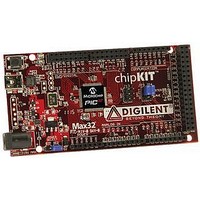
ChipKIT Max32 Development Board PIC32 Boards And Kits
Manufacturer
Microchip Technology
Series
PIC® 32MXr
Type
MCUr
Specifications of TDGL003
Silicon Manufacturer
Microchip
Core Architecture
MIPS
Core Sub-architecture
PIC32
Silicon Core Number
PIC32MX
Silicon Family Name
PIC32MX795Fxxxx
Kit Contents
Board Only
Contents
Board
Lead Free Status / Rohs Status
Lead free / RoHS Compliant
For Use With/related Products
MPLAB®, Arduino™ Mega


22.0
The
Converter (ADC) includes the following features:
• Successive Approximation Register (SAR)
• Up to 1000 kilo samples per second (ksps)
• Up to 16 analog input pins
• External voltage reference input pins
• One unipolar, differential Sample-and-Hold
FIGURE 22-1:
© 2011 Microchip Technology Inc.
conversion
conversion speed
Amplifier (SHA)
Note 1: This data sheet summarizes the features
Note
CH0SA<4:0>
CHANNEL
PIC32MX3XX/4XX
SCAN
2: Some registers and associated bits
1:
CONVERTER (ADC)
10-BIT ANALOG-TO-DIGITAL
of the PIC32MX3XX/4XX family of
devices. It is not intended to be a compre-
hensive reference source. Refer to Sec-
tion
Converter (ADC)” (DS61104) of the
“PIC32 Family Reference Manual”, which
is available from the Microchip web site
(www.microchip.com/PIC32).
described in this section may not be
available on all devices. Refer to
Section 4.0 “Memory Organization”
this data sheet for device-specific register
and bit information.
V
V
REF
REFL
AN1
AN15
+, V
AN0
CH0NA CH0NB
CSCNA
17.
REF
- inputs can be multiplexed with other analog inputs.
ADC1 MODULE BLOCK DIAGRAM
“10-bit
CH0SB<4:0>
10-bit
Input Selection
Alternate
Analog-to-Digital
Analog-to-Digital
+
-
in
• Automatic Channel Scan mode
• Selectable conversion trigger source
• 16-word conversion result buffer
• Selectable Buffer Fill modes
• Eight conversion result format options
• Operation during CPU Sleep and Idle modes
A block diagram of the 10-bit ADC is illustrated in
Figure
designated AN0-AN15. In addition, there are two ana-
log input pins for external voltage reference connec-
tions. These voltage reference inputs may be shared
with other analog input pins and may be common to
other analog module references.
The analog inputs are connected through two multi-
plexers (MUXs) to one SHA. The analog input MUXs
can be switched between two sets of analog inputs
between conversions. Unipolar differential conversions
are possible on all
the reference, using a reference input pin (see
Figure
The Analog Input Scan mode sequentially converts
user-specified channels. A control register specifies
which analog input channels will be included in the
scanning sequence.
The 10-bit ADC is connected to a 16-word result buffer.
Each 10-bit result is converted to one of eight, 32-bit
output formats when it is read from the result buffer.
S/H
22-1. The 10-bit ADC has 16 analog input pins,
22-1).
PIC32MX3XX/4XX
V
REF
+
V
(1)
REFH
channels,
AV
VCFG<2:0>
SAR ADC
DD
V
REF
other than the pin used as
V
-
REFL
(1)
AV
DS61143H-page 123
SS
ADC1BUFE
ADC1BUFF
ADC1BUF0
ADC1BUF1
ADC1BUF2
Related parts for TDGL003
Image
Part Number
Description
Manufacturer
Datasheet
Request
R

Part Number:
Description:
Manufacturer:
Microchip Technology Inc.
Datasheet:
Part Number:
Description:
Manufacturer:
Microchip Technology Inc.
Datasheet:
Part Number:
Description:
Manufacturer:
Microchip Technology Inc.
Datasheet:
Part Number:
Description:
Manufacturer:
Microchip Technology Inc.
Datasheet:
Part Number:
Description:
Manufacturer:
Microchip Technology Inc.
Datasheet:
Part Number:
Description:
Manufacturer:
Microchip Technology Inc.
Datasheet:
Part Number:
Description:
Manufacturer:
Microchip Technology Inc.
Datasheet:
Part Number:
Description:
Manufacturer:
Microchip Technology Inc.
Datasheet: