TDGL003 Microchip Technology, TDGL003 Datasheet - Page 69
TDGL003
Manufacturer Part Number
TDGL003
Description
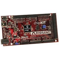
ChipKIT Max32 Development Board PIC32 Boards And Kits
Manufacturer
Microchip Technology
Series
PIC® 32MXr
Type
MCUr
Specifications of TDGL003
Silicon Manufacturer
Microchip
Core Architecture
MIPS
Core Sub-architecture
PIC32
Silicon Core Number
PIC32MX
Silicon Family Name
PIC32MX795Fxxxx
Kit Contents
Board Only
Contents
Board
Lead Free Status / Rohs Status
Lead free / RoHS Compliant
For Use With/related Products
MPLAB®, Arduino™ Mega


TABLE 4-19:
TABLE 4-20:
Legend:
Note
Legend:
Note
F400 NVMCON
F410
F420 NVMADDR
F430 NVMDATA
F440
F000 OSCCON
F010 OSCTUN
F600
F610 RSWRST
F230 SYSKEY
0000 WDTCON
1:
1:
2:
3:
NVMSRC
NVMKEY
RCON
ADDR
x = unknown value on Reset, — = unimplemented, read as ‘0’. Reset values are shown in hexadecimal.
This register has corresponding CLR, SET and INV registers at its virtual address, plus an offset of 0x4, 0x8 and 0xC, respectively. See
x = unknown value on Reset, — = unimplemented, read as ‘0’. Reset values are shown in hexadecimal.
Except where noted, all registers in this table have corresponding CLR, SET and INV registers at their virtual addresses, plus offsets of 0x4, 0x8 and 0xC, respectively. See
Registers”
Reset values are dependent on the DEVCFGx Configuration bits and the type of reset.
This register does not have associated CLR, SET, and INV registers.
(3)
(1)
(1)
31:16
31:16
31:16
31:16
31:16
31:16
15:0
15:0
15:0
15:0
15:0
15:0
31:16
31:16
31:16
31:16
31:16
15:0
15:0
15:0
15:0
15:0
FLASH CONTROLLER REGISTERS MAP
SYSTEM CONTROL REGISTERS MAP
for more information.
31/15
31/15
ON
—
—
—
—
—
—
—
—
—
WR
—
30/14
WREN
30/14
—
—
—
—
—
—
—
—
—
—
COSC<2:0>
29/13
WRERR
29/13
—
—
—
—
—
—
—
—
—
PLLODIV<2:0>
28/12
LVDERR
28/12
—
—
—
—
—
—
—
—
—
LVDSTAT
27/11
27/11
—
—
—
—
—
—
—
—
—
—
(1,2)
26/10
26/10
—
—
—
—
—
—
—
—
—
—
FRCDIV<2:0>
NOSC<2:0>
CMR
25/9
25/9
—
—
—
—
—
—
—
—
—
NVMSRCADDR<31:0>
VREGS
NVMADDR<31:0>
24/8
NVMDATA<31:0>
SYSKEY<31:0>
NVMKEY<31:0>
24/8
—
—
—
—
—
—
—
—
—
Bits
Bits
CLKLOCK
EXTR
23/7
23/7
—
—
—
—
—
—
—
—
—
—
SOSCRDY
ULOCK
SWR
22/6
22/6
—
—
—
—
—
—
—
—
Section 12.1.1 “CLR, SET and INV Registers”
SLOCK
21/5
21/5
—
—
—
—
—
—
—
—
—
SWDTPS<4:0>
SLPEN
WDTO
20/4
20/4
—
—
—
—
—
—
—
PBDIV<1:0>
SLEEP
19/3
19/3
CF
—
—
—
—
—
—
TUN<5:0>
UFRCEN
Section 12.1.1 “CLR, SET and INV
IDLE
18/2
18/2
—
—
—
—
—
—
NVMOP<3:0>
PLLMULT<2:0>
SOSCEN
for more information.
17/1
BOR
17/1
—
—
—
—
—
—
—
WDTCLR 0000
OSWEN
SWRST
POR
16/0
16/0
—
—
—
—
—
0000
0000
0000
0000
0000
0000
0000
0000
0000
0000
0000
0000
0000
0000
0000
0000
0000
0000
0000
0000
0000
Related parts for TDGL003
Image
Part Number
Description
Manufacturer
Datasheet
Request
R

Part Number:
Description:
Manufacturer:
Microchip Technology Inc.
Datasheet:
Part Number:
Description:
Manufacturer:
Microchip Technology Inc.
Datasheet:
Part Number:
Description:
Manufacturer:
Microchip Technology Inc.
Datasheet:
Part Number:
Description:
Manufacturer:
Microchip Technology Inc.
Datasheet:
Part Number:
Description:
Manufacturer:
Microchip Technology Inc.
Datasheet:
Part Number:
Description:
Manufacturer:
Microchip Technology Inc.
Datasheet:
Part Number:
Description:
Manufacturer:
Microchip Technology Inc.
Datasheet:
Part Number:
Description:
Manufacturer:
Microchip Technology Inc.
Datasheet: