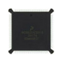
DSP56002FC66 Freescale Semiconductor, DSP56002FC66 Datasheet - Page 103

DSP56002FC66
Manufacturer Part Number
DSP56002FC66
Description
Manufacturer
Freescale Semiconductor
Datasheet
1.DSP56002FC66.pdf
(110 pages)
Specifications of DSP56002FC66
Device Core Size
24b
Architecture
Harvard
Format
Fixed Point
Clock Freq (max)
66MHz
Mips
33
Device Input Clock Speed
66MHz
Ram Size
3KB
Program Memory Size
1.5KB
Operating Supply Voltage (typ)
5V
Operating Supply Voltage (min)
4.5V
Operating Supply Voltage (max)
5.5V
Operating Temp Range
-40C to 105C
Operating Temperature Classification
Industrial
Mounting
Surface Mount
Pin Count
132
Package Type
PQFP
Lead Free Status / Rohs Status
Supplier Unconfirmed
Available stocks
Company
Part Number
Manufacturer
Quantity
Price
Company:
Part Number:
DSP56002FC66
Manufacturer:
MOTOROLA
Quantity:
5 530
Company:
Part Number:
DSP56002FC66
Manufacturer:
MOTOROLA
Quantity:
6 250
Company:
Part Number:
DSP56002FC66
Manufacturer:
MOTOROLA
Quantity:
591
Part Number:
DSP56002FC66
Manufacturer:
MOTOROLA/摩托罗拉
Quantity:
20 000
Company:
Part Number:
DSP56002FC661H72G
Manufacturer:
AD
Quantity:
92
ELECTRICAL DESIGN CONSIDERATIONS
MOTOROLA
Use the following list of recommendations to assure correct DSP operation:
• Provide a low-impedance path from the board power supply to each V
• Use at least four 0.1 F bypass capacitors positioned as close as possible to the
• Ensure that capacitor leads and associated printed circuit traces that connect
• Use at least a four-layer Printed Circuit Board (PCB) with two inner layers for
• Because the DSP output signals have fast rise and fall times, PCB trace lengths
• Consider all device loads as well as parasitic capacitance due to PCB traces
• All inputs must be terminated (i.e., not allowed to float) using CMOS levels.
• Take special care to minimize noise levels on the PLL supply pins (both V
on the DSP, and from the board ground to each GND pin.
four sides of the package to connect the V
to the chip V
V
should be minimal. This recommendation particularly applies to the address
and data buses as well as the RD, WR, IRQA, IRQB, NMI, HEN, and HACK
pins.
when calculating capacitance. This is especially critical in systems with higher
capacitive loads that could create higher transient currents in the V
GND circuits.
and GND).
CC
Freescale Semiconductor, Inc.
and GND.
This device contains protective circuitry to
guard against damage due to high static
voltage or electrical fields. However, normal
precautions are advised to avoid application
of any voltages higher than maximum rated
voltages to this high-impedance circuit.
Reliability of operation is enhanced if unused
inputs are tied to an appropriate logic voltage
level (e.g., either GND or V
For More Information On This Product,
CC
Go to: www.freescale.com
and GND pins are less than 0.5 inch per capacitor lead.
DSP56002/D, Rev. 3
CAUTION
CC
).
CC
power source to GND.
Electrical Design Considerations
Design Considerations
CC
and
CC
CC
pin
4-3


