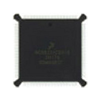
DSP56002FC66 Freescale Semiconductor, DSP56002FC66 Datasheet - Page 55

DSP56002FC66
Manufacturer Part Number
DSP56002FC66
Description
Manufacturer
Freescale Semiconductor
Datasheet
1.DSP56002FC66.pdf
(110 pages)
Specifications of DSP56002FC66
Device Core Size
24b
Architecture
Harvard
Format
Fixed Point
Clock Freq (max)
66MHz
Mips
33
Device Input Clock Speed
66MHz
Ram Size
3KB
Program Memory Size
1.5KB
Operating Supply Voltage (typ)
5V
Operating Supply Voltage (min)
4.5V
Operating Supply Voltage (max)
5.5V
Operating Temp Range
-40C to 105C
Operating Temperature Classification
Industrial
Mounting
Surface Mount
Pin Count
132
Package Type
PQFP
Lead Free Status / Rohs Status
Supplier Unconfirmed
Available stocks
Company
Part Number
Manufacturer
Quantity
Price
Company:
Part Number:
DSP56002FC66
Manufacturer:
MOTOROLA
Quantity:
5 530
Company:
Part Number:
DSP56002FC66
Manufacturer:
MOTOROLA
Quantity:
6 250
Company:
Part Number:
DSP56002FC66
Manufacturer:
MOTOROLA
Quantity:
591
Part Number:
DSP56002FC66
Manufacturer:
MOTOROLA/摩托罗拉
Quantity:
20 000
Company:
Part Number:
DSP56002FC661H72G
Manufacturer:
AD
Quantity:
92
EXTERNAL BUS SYNCHRONOUS TIMING
C
Capacitance Derating: The DSP56002 external bus timing specifications are designed and tested
at the maximum capacitive load of 50 pF, including stray capacitance. Typically, the drive
capability of the external bus pins (A0–A15, D0–D23, PS, DS, RD, WR, X/Y) derates linearly at 1
ns per 12 pF of additional capacitance from 50 pF to 250 pF of loading. Port B and C pins (HI,
SCI, SSI, and Timer) derate linearly at 1 ns per 5 pF of additional capacitance from 50 pF to 250
pF of loading. Active-low lines should be “pulled up” in a manner consistent with the ac and dc
specifications.
MOTOROLA
Num
Notes:
140 First CKOUT transition to Address Valid
141 Second CKOUT transition to WR
142 Second CKOUT transition to WR
143 Second CKOUT transition to RD
144 Second CKOUT transition to RD
145 First CKOUT transition to Data-Out Valid
146 First CKOUT transition to Data-Out
147 Data-In Valid to second CKOUT transition
148 Second CKOUT transition to Data-In
149 First CKOUT transition to Address
L
= 50 pF + 2 TTL loads
Assertion
Deassertion
Assertion
Deassertion
Invalid
(Setup)
Invalid (Hold)
Invalid
1.
2.
3.
4.
5.
•
•
AC timing specifications which are referenced to a device input signal are measured in production
with respect to the 50% point of the respective input signal’s transition.
WS are wait state values specified in the BCR.
First CKOUT transition to data-out invalid (specification # T146) and first CKOUT transition to
address invalid (specification # T149) indicate the time after which data/address are no longer
guaranteed to be valid.
Timings are given from CKOUT midpoint to V
First CKOUT transition is a falling edge of CKOUT for CKP = 0.
3
3
WS = 0
WS > 0
1
Characteristics
Freescale Semiconductor, Inc.
For More Information On This Product,
Table 2-13 External Bus Synchronous Timing
Go to: www.freescale.com
DSP56002/D, Rev. 3
Min
1.3
3.4
—
—
—
—
—
0
0
0
0
40 MHz
OL
T
or V
H
Max
6.2
4.4
9.1
3.9
3.4
5.4
—
—
—
—
+ 4.4
OH
of the corresponding pin(s).
Min
3.4
External Bus Synchronous Timing
—
—
—
—
–3
—
1
0
0
0
66 MHz
T
Max
H
3.9
4.5
—
—
—
—
5
4
5
3
+ 4
Min
3.4
—
—
—
—
–3
—
1
0
0
0
80 MHz
Specifications
T
Max
H
3.9
4.5
—
—
—
—
5
4
5
3
+ 4
Unit
2-29
ns
ns
ns
ns
ns
ns
ns
ns
ns
ns
ns


