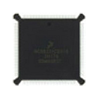
DSP56002FC66 Freescale Semiconductor, DSP56002FC66 Datasheet - Page 62

DSP56002FC66
Manufacturer Part Number
DSP56002FC66
Description
Manufacturer
Freescale Semiconductor
Datasheet
1.DSP56002FC66.pdf
(110 pages)
Specifications of DSP56002FC66
Device Core Size
24b
Architecture
Harvard
Format
Fixed Point
Clock Freq (max)
66MHz
Mips
33
Device Input Clock Speed
66MHz
Ram Size
3KB
Program Memory Size
1.5KB
Operating Supply Voltage (typ)
5V
Operating Supply Voltage (min)
4.5V
Operating Supply Voltage (max)
5.5V
Operating Temp Range
-40C to 105C
Operating Temperature Classification
Industrial
Mounting
Surface Mount
Pin Count
132
Package Type
PQFP
Lead Free Status / Rohs Status
Supplier Unconfirmed
Available stocks
Company
Part Number
Manufacturer
Quantity
Price
Company:
Part Number:
DSP56002FC66
Manufacturer:
MOTOROLA
Quantity:
5 530
Company:
Part Number:
DSP56002FC66
Manufacturer:
MOTOROLA
Quantity:
6 250
Company:
Part Number:
DSP56002FC66
Manufacturer:
MOTOROLA
Quantity:
591
Part Number:
DSP56002FC66
Manufacturer:
MOTOROLA/摩托罗拉
Quantity:
20 000
Company:
Part Number:
DSP56002FC661H72G
Manufacturer:
AD
Quantity:
92
Specifications
OnCE Port Timing
OnCE PORT TIMING
C
2-36
L
Num
250A
230
231
232
233
234
235
236
237
238
239
240
241
242
243
244
245
246
247
248
249
= 50 pF + 2 TTL loads
DSCK Low
DSCK High
DSCK Cycle Time
DR Asserted to DSO (ACK) Asserted
DSCK High to DSO Valid
DSCK High to DSO Invalid
DSI Valid to DSCK Low (Setup)
DSCK Low to DSI Invalid (Hold)
Last DSCK Low to OS0–OS1, ACK Active
DSO (ACK) Asserted to First DSCK High
DSO (ACK) Assertion Width
DSO (ACK) Asserted to OS0–OS1 High Impedance
OS0–OS1 Valid to second CKOUT transition
Second CKOUT transition to OS0–OS1 Invalid
Last DSCK Low of Read Register to First DSCK
High of Next Command
Last DSCK Low to DSO Invalid (Hold)
DR Assertion to second CKOUT transition for Wake
Up from Wait state
Second CKOUT transition to DSO after Wake Up
from Wait state
DR Assertion Width
DR Assertion to DSO (ACK) Valid (enter Debug
mode) After Asynchronous Recovery from Wait State
DR Assertion Width to Recover from Stop state
•
•
•
•
•
To recover from Wait state
To recover from Wait state and enter Debug
mode
Stable External Clock, OMR Bit 6 = 0
Stable External Clock, OMR Bit 6 = 1
Stable External Clock, PCTL Bit 17= 1
Characteristics
Freescale Semiconductor, Inc.
For More Information On This Product,
Table 2-15 OnCE Port Timing
DSP56002/D, Rev. 3
Go to: www.freescale.com
1
2
4T
13T
3T
7T
C
T
17T
17T
Min
C
5T
C
2T
+ T
200
C
40
40
—
15
—
12
15
C
15
15
15
3
3
0
3
– 21
+ T
+ 10
C
C
+ 15
C
C
H
L
– 3
65548T
20T
13T
12T
5T
Max
T
C
C
—
—
—
—
42
—
—
—
—
—
C
—
—
—
—
—
—
—
C
0
C
C
+ 7
+ T
+ T
– 15
MOTOROLA
+ T
L
L
L
Unit
ns
ns
ns
ns
ns
ns
ns
ns
ns
ns
ns
ns
ns
ns
ns
ns
ns
ns
ns
ns
ns
ns
ns


