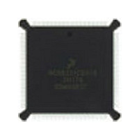
DSP56002FC66 Freescale Semiconductor, DSP56002FC66 Datasheet - Page 11

DSP56002FC66
Manufacturer Part Number
DSP56002FC66
Description
Manufacturer
Freescale Semiconductor
Datasheet
1.DSP56002FC66.pdf
(110 pages)
Specifications of DSP56002FC66
Device Core Size
24b
Architecture
Harvard
Format
Fixed Point
Clock Freq (max)
66MHz
Mips
33
Device Input Clock Speed
66MHz
Ram Size
3KB
Program Memory Size
1.5KB
Operating Supply Voltage (typ)
5V
Operating Supply Voltage (min)
4.5V
Operating Supply Voltage (max)
5.5V
Operating Temp Range
-40C to 105C
Operating Temperature Classification
Industrial
Mounting
Surface Mount
Pin Count
132
Package Type
PQFP
Lead Free Status / Rohs Status
Supplier Unconfirmed
Available stocks
Company
Part Number
Manufacturer
Quantity
Price
Company:
Part Number:
DSP56002FC66
Manufacturer:
MOTOROLA
Quantity:
5 530
Company:
Part Number:
DSP56002FC66
Manufacturer:
MOTOROLA
Quantity:
6 250
Company:
Part Number:
DSP56002FC66
Manufacturer:
MOTOROLA
Quantity:
591
Part Number:
DSP56002FC66
Manufacturer:
MOTOROLA/摩托罗拉
Quantity:
20 000
Company:
Part Number:
DSP56002FC661H72G
Manufacturer:
AD
Quantity:
92
PLL AND CLOCK
MOTOROLA
EXTAL
XTAL
CKOUT
CKP
PCAP
Signal
Name
Output
Output
Output
Input/
Signal
Input
Input
Type
Freescale Semiconductor, Inc.
Indeter-
during
minate
driven
driven
Reset
Input
Chip-
Chip-
Input
State
For More Information On This Product,
Table 1-4 PLL and Clock Signals
Go to: www.freescale.com
External Clock/Crystal Input—This input connects the internal
oscillator input to an external crystal or to an external oscillator.
Crystal Output—This output connects the internal crystal oscillator
output to an external crystal. If an external oscillator is used, XTAL
should be left unconnected.
PLL Output Clock—When the PLL is enabled and locked, this
signal provides a 50% duty cycle output clock signal synchronized
to the internal processor clock.
When the PLL is enabled and the Multiplication Factor is less than
or equal to 4, then CKOUT is synchronized to EXTAL.
When the PLL is disabled, the output clock at CKOUT is derived
from, and has the same frequency and duty cycle as, EXTAL.
Note:
PLL Output Clock Polarity Control—The value of this signal at
reset defines the polarity of the CKOUT output relative to EXTAL. If
CKP is pulled low by connecting through a resistor to ground,
CKOUT and EXTAL have the same polarity. Pulling CKP high by
connecting it through a resistor to V
to be inverse polarities. The polarity of CKOUT is latched at the end
of reset; therefore, any changes to CKP after deassertion of RESET
do not affect CKOUT polarity.
PLL Capacitor—This signal is used to connect the required external
filter capacitor to the PLL filter. Connect one end of the capacitor to
PCAP and the other to V
in Section 2 of this data sheet.
DSP56002/D, Rev. 3
For information about using the PLL Multiplication Factor,
see the
DSP56002 User’s Manual
Signal Description
CCP
. The value of the capacitor is specified
CC
causes CKOUT and EXTAL
.
Signal/Pin Descriptions
PLL and Clock
1-5


