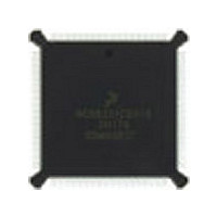
DSP56002FC66 Freescale Semiconductor, DSP56002FC66 Datasheet - Page 24

DSP56002FC66
Manufacturer Part Number
DSP56002FC66
Description
Manufacturer
Freescale Semiconductor
Datasheet
1.DSP56002FC66.pdf
(110 pages)
Specifications of DSP56002FC66
Device Core Size
24b
Architecture
Harvard
Format
Fixed Point
Clock Freq (max)
66MHz
Mips
33
Device Input Clock Speed
66MHz
Ram Size
3KB
Program Memory Size
1.5KB
Operating Supply Voltage (typ)
5V
Operating Supply Voltage (min)
4.5V
Operating Supply Voltage (max)
5.5V
Operating Temp Range
-40C to 105C
Operating Temperature Classification
Industrial
Mounting
Surface Mount
Pin Count
132
Package Type
PQFP
Lead Free Status / Rohs Status
Supplier Unconfirmed
Available stocks
Company
Part Number
Manufacturer
Quantity
Price
Company:
Part Number:
DSP56002FC66
Manufacturer:
MOTOROLA
Quantity:
5 530
Company:
Part Number:
DSP56002FC66
Manufacturer:
MOTOROLA
Quantity:
6 250
Company:
Part Number:
DSP56002FC66
Manufacturer:
MOTOROLA
Quantity:
591
Part Number:
DSP56002FC66
Manufacturer:
MOTOROLA/摩托罗拉
Quantity:
20 000
Company:
Part Number:
DSP56002FC661H72G
Manufacturer:
AD
Quantity:
92
Signal/Pin Descriptions
On-Chip Emulation Port
On-CHIP EMULATION PORT
1-18
Signal Name
DSI/OS0
DSCK/OS1
Output
Output
Signal
Input
Input
Type
or
or
Table 1-13 On-Chip Emulation (OnCE) Signals
Output
Output
during
Reset
State
Low
Low
Freescale Semiconductor, Inc.
For More Information On This Product,
Debug Serial Input/Chip Status 0—Serial data or commands
are provided to the OnCE controller through the DSI/OS0 signal
when it is an input. The data received on the DSI signal will be
recognized only when the DSP has entered the Debug mode of
operation. Data is latched on the falling edge of the DSCK serial
clock. Data is always shifted into the OnCE serial port Most
Significant Bit (MSB) first. When the DSI/OS0 signal is an
output, it works in conjunction with the OS1 signal to provide
chip status information. The DSI/OS0 signal is an output when
the processor is not in Debug mode. When switching from
output to input, the signal is tri-stated.
Note:
Debug Serial Clock/Chip Status 1—The DSCK/OS1 signal
supplies the serial clock to the OnCE when it is an input. The
serial clock provides pulses required to shift data into and out of
the OnCE serial port. (Data is clocked into the OnCE on the
falling edge and is clocked out of the OnCE serial port on the
rising edge.) The debug serial clock frequency must be no
greater than
switching from input to output, the signal is tri-stated.
When it is an output, this signal works with the OS0 signal to
provide information about the chip status. The DSCK/OS1 signal
is an output when the chip is not in Debug mode.
Note:
DSP56002/D, Rev. 3
Go to: www.freescale.com
Connect an external pull-down resistor to this signal.
Connect an external pull-down resistor to this signal.
1
/
8
of the processor clock frequency. When
Signal Description
MOTOROLA


