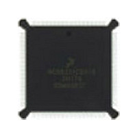
DSP56002FC66 Freescale Semiconductor, DSP56002FC66 Datasheet - Page 15

DSP56002FC66
Manufacturer Part Number
DSP56002FC66
Description
Manufacturer
Freescale Semiconductor
Datasheet
1.DSP56002FC66.pdf
(110 pages)
Specifications of DSP56002FC66
Device Core Size
24b
Architecture
Harvard
Format
Fixed Point
Clock Freq (max)
66MHz
Mips
33
Device Input Clock Speed
66MHz
Ram Size
3KB
Program Memory Size
1.5KB
Operating Supply Voltage (typ)
5V
Operating Supply Voltage (min)
4.5V
Operating Supply Voltage (max)
5.5V
Operating Temp Range
-40C to 105C
Operating Temperature Classification
Industrial
Mounting
Surface Mount
Pin Count
132
Package Type
PQFP
Lead Free Status / Rohs Status
Supplier Unconfirmed
Available stocks
Company
Part Number
Manufacturer
Quantity
Price
Company:
Part Number:
DSP56002FC66
Manufacturer:
MOTOROLA
Quantity:
5 530
Company:
Part Number:
DSP56002FC66
Manufacturer:
MOTOROLA
Quantity:
6 250
Company:
Part Number:
DSP56002FC66
Manufacturer:
MOTOROLA
Quantity:
591
Part Number:
DSP56002FC66
Manufacturer:
MOTOROLA/摩托罗拉
Quantity:
20 000
Company:
Part Number:
DSP56002FC661H72G
Manufacturer:
AD
Quantity:
92
MOTOROLA
BN
WT
WR
RD
Signal
Name
Output Pulled
Output Tri-stated Write Enable—WR is asserted low during external memory write
Output Tri-stated Read Enable—RD is asserted low during external memory read
Signal
Input
Type
low
Input
during
Freescale Semiconductor, Inc.
Reset
State
For More Information On This Product,
Table 1-7 Bus Control Signals (Continued)
Bus Not Required—The BN signal is asserted whenever the chip
requires mastership of the external bus. During instruction cycles
where the external bus is not required, BN is deasserted. If the BN
signal is asserted when the DSP is not the bus master, processing has
stopped and the chip is waiting to acquire bus ownership. An external
arbiter may use this signal to help determine when to return bus
ownership to the DSP.
Note:
Bus Wait—An external device may insert wait states by asserting WT
during external bus cycles.
Note:
cycles. WR is tri-stated when the BG or RESET signal is asserted.
cycles. RD is tri-stated when the BG or RESET signal is asserted.
Go to: www.freescale.com
DSP56002/D, Rev. 3
The BN signal cannot be used as an early indication of
imminent external bus access because it is valid later than the
other bus control signals BS and WT.
To prevent erroneous operation, pull up the WT signal when
it is not in use.
Signal Description
Signal/Pin Descriptions
Bus Control
1-9


