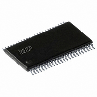
SC28L201A1DGG,112 NXP Semiconductors, SC28L201A1DGG,112 Datasheet - Page 46

SC28L201A1DGG,112
Manufacturer Part Number
SC28L201A1DGG,112
Description
IC UART W/FIFO 48-TSSOP
Manufacturer
NXP Semiconductors
Series
IMPACTr
Datasheet
1.SC28L201A1DGG118.pdf
(110 pages)
Specifications of SC28L201A1DGG,112
Features
False-start Bit Detection
Number Of Channels
2, DUART
Fifo's
256 Byte
Voltage - Supply
3.3V, 5V
With Parallel Port
Yes
With Auto Flow Control
Yes
With False Start Bit Detection
Yes
With Modem Control
Yes
With Cmos
Yes
Mounting Type
Surface Mount
Package / Case
48-TSSOP
Lead Free Status / RoHS Status
Lead free / RoHS Compliant
Other names
568-3293-5
935277824112
SC28L201A1DGG
935277824112
SC28L201A1DGG
Philips Semiconductors
9397 750 13138
Product data sheet
8.2.3 Mode Register 2 (MR2)
MR2 can be accessed directly at 0x22 in the Extended section of the address map, or by
means of the MR Pointer at 0x00 used by legacy code.
The MR2 register provides basic channel setup control that may need more frequent
updating.
Table 18:
Bit
7:6
Symbol
MR2 - Mode Register 2 (address 0x22) bit description
Description
Channel Mode Select. The UART can operate in one of the following four
modes:
Normal mode: the transmitter and receiver operating independently.
Automatic Echo mode: this mode automatically retransmits the received
data. The following conditions are true while in Automatic Echo mode:
Local loopback mode. In this mode:
Remote Loopback diagnostic mode. In this mode:
•
•
•
•
•
•
•
•
•
•
•
•
•
•
•
•
•
•
•
•
•
00 = Normal mode (default)
01 = Automatic Echo mode
10 = Local loopback mode
11 = Remote loopback mode
Rev. 01 — 31 October 2005
Received data is re-clocked and re-transmitted on the TXD output.
The receiver clock is used for the transmitted data.
The receiver must be enabled, but the transmitter need not be enabled.
The TxRDY and Tx Idle status bits are inactive.
The received parity is checked, but is not regenerated for transmission,
that is, transmitted parity bit is as received.
Character framing is checked, but the stop bits are retransmitted as
received. Rx data is sent to RxFIFO.
A received break is echoed as received until the next valid start bit is
detected.
CPU to receiver communication continues normally, but the CPU to
transmitter link is disabled.
The transmitter output is internally connected to the receiver input.
The transmitter’s 1 clock is used for the receiver.
The TXD output is held HIGH.
The RXD input is ignored.
The transmitter must be enabled, but the receiver need not be enabled.
CPU to transmitter and receiver communications continue normally.
Received data is re-clocked and re-transmitted on the TXD output.
The receiver 1 clock is used for the transmitted data.
Received data is not sent to the local CPU, and the error status
conditions are inactive.
The received parity is not checked and is not regenerated for
transmission, that is, the transmitted parity bit is as received.
The receiver must be enabled, but the transmitter need not be enabled.
Character framing is not checked, and the stop bits are retransmitted as
received.
A received break is echoed as received until the next valid start bit is
detected.
3.3 V, 5 V UART, 3.125 Mbit/s, with 256-byte FIFO
© Koninklijke Philips Electronics N.V. 2005. All rights reserved.
SC28L201
46 of 110


