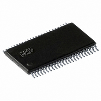
SC28L201A1DGG,112 NXP Semiconductors, SC28L201A1DGG,112 Datasheet - Page 7

SC28L201A1DGG,112
Manufacturer Part Number
SC28L201A1DGG,112
Description
IC UART W/FIFO 48-TSSOP
Manufacturer
NXP Semiconductors
Series
IMPACTr
Datasheet
1.SC28L201A1DGG118.pdf
(110 pages)
Specifications of SC28L201A1DGG,112
Features
False-start Bit Detection
Number Of Channels
2, DUART
Fifo's
256 Byte
Voltage - Supply
3.3V, 5V
With Parallel Port
Yes
With Auto Flow Control
Yes
With False Start Bit Detection
Yes
With Modem Control
Yes
With Cmos
Yes
Mounting Type
Surface Mount
Package / Case
48-TSSOP
Lead Free Status / RoHS Status
Lead free / RoHS Compliant
Other names
568-3293-5
935277824112
SC28L201A1DGG
935277824112
SC28L201A1DGG
Philips Semiconductors
Table 2:
See
9397 750 13138
Product data sheet
Symbol
RDN
A6 to A0
RESET
IRQN
IACKN
X1/SCLK
X2
RXD
TXD
I/O7A to I/O0A
I/O6B
I/O4B to I/O2B
I/O0B
V
V
DD
SS
Figure
3.
Pin description for 80xxx bus interface (Intel)
Pin
28
3, 4, 5, 6,
20, 21, 22
8
46
23
47
48
7
45
37, 38, 39,
40, 41, 42,
43, 44
29
30, 31, 32
33
1, 13, 24,
34
2, 14, 25,
35, 36
Type
I
I
I
O
I
I
O
I
O
I/O
I/O
power
power
Description
Read strobe. When LOW and CEN is also LOW, causes the contents of the
addressed register to be presented on the data bus. The read cycle begins on the
falling edge of RDN.
Address inputs. Select the UART internal registers and ports for read/write
operations.
Reset. A HIGH level clears internal registers (SR, IMR, ISR, OPR, OPCR), places
I/O[7:0] at high-impedance input state, stops the counter/timer, and puts Channel in
the inactive state, with the TXD output in the ‘mark’ (HIGH) state. Sets MR pointer to
MR1 9600 baud, 1 start, no parity and 1 stop bit(s).
Interrupt request. Active LOW, open-drain output which signals the CPU that one
or more of the eleven (11) maskable interrupting conditions are true.
Interrupt acknowledge. Active LOW input indicates an interrupt acknowledge
cycle. Usually asserted by the CPU in response to an interrupt request. When
asserted places the interrupt vector on the bus.
Crystal 1. Crystal or external clock input. A crystal or clock of the specified limits
must be supplied at all times. When a crystal is used, a capacitor must be connected
from this pin to ground (see Figure 12).
Crystal 2. Connection for other side of the crystal. When a crystal is used, a
capacitor must be connected from this pin to ground (see Figure 12). If X1/SCLK is
driven from an external source, this pin must be open or not driving more than
2 CMOS or TTL loads.
Channel A Receiver serial data input. The least significant bit is received first.
‘Mark’ is HIGH; ‘space’ is LOW.
Channel A Transmitter serial data output. The least significant bit is transmitted
first. This output is held in the ‘mark’ condition when the transmitter is disabled, idle
or when operating in local loopback mode. ‘Mark’ is HIGH; ‘space’ is LOW.
General-purpose input and output ports. The character of these pins is controlled
by I/OPCR. They may be inputs or outputs and will present many internal clocks and
interrupt signals: RTS, CTS, DTR, DSR, and so on. All have change-of-state
detectors and the input is always active. These pins are set to input only when
addressed from the low order address space. When these pins are configured for
interrupt type signals (RXRDY, TXRDY, C/TRDY), they switch to open-drain outputs.
Each of these pins has a small pull-up ‘resistor’ that supplies approximately 5 A of
current.
Additional general-purpose I/O pins. They are similar to the above without any
connection to the data path or clocks. They have Change-Of-State (COS) detectors
and will generate interrupts if enabled. Each of these pins has a small pull-up
‘resistor’ that supplies approximately 5 A of current.
Power supply (4 pins). +3.3 V
assured from 2.97 V or 5.5 V. Timing parameters are specified with respect to the
V
Ground (5 pins)
DD
being at 3.3 V
Rev. 01 — 31 October 2005
10 % or 5.0 V
…continued
3.3 V, 5 V UART, 3.125 Mbit/s, with 256-byte FIFO
10 % or +5.0 V
10 %.
© Koninklijke Philips Electronics N.V. 2005. All rights reserved.
10 % supply input. Operation is
SC28L201
7 of 110


