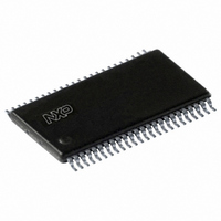
SC28L201A1DGG,112 NXP Semiconductors, SC28L201A1DGG,112 Datasheet - Page 67

SC28L201A1DGG,112
Manufacturer Part Number
SC28L201A1DGG,112
Description
IC UART W/FIFO 48-TSSOP
Manufacturer
NXP Semiconductors
Series
IMPACTr
Datasheet
1.SC28L201A1DGG118.pdf
(110 pages)
Specifications of SC28L201A1DGG,112
Features
False-start Bit Detection
Number Of Channels
2, DUART
Fifo's
256 Byte
Voltage - Supply
3.3V, 5V
With Parallel Port
Yes
With Auto Flow Control
Yes
With False Start Bit Detection
Yes
With Modem Control
Yes
With Cmos
Yes
Mounting Type
Surface Mount
Package / Case
48-TSSOP
Lead Free Status / RoHS Status
Lead free / RoHS Compliant
Other names
568-3293-5
935277824112
SC28L201A1DGG
935277824112
SC28L201A1DGG
Philips Semiconductors
9397 750 13138
Product data sheet
8.4.7 Counter/Timer Preset Upper and Counter/Timer Preset Lower (CTPU, CTPL)
Table 43:
Table 44:
Table 45:
The CTPU and CTPL hold the eight MSBs and eight LSBs, respectively, of the value to be
used by the Counter/Timer in either the counter or timer modes of operation. The
minimum value that may be loaded into the CTPU/CTPL registers is 0x0000. Note that
these registers are write-only and cannot be read by the CPU.
In the timer mode, the C/T generates a square wave whose period is twice the value (in
C/T clock periods) of the CTPU and CTPL. The waveform so generated is often used for a
data clock. The formula for calculating the divisor ‘n’ to load to the CTPU and CTPL for a
particular 1 data clock is shown in
Remark: The 2 in the denominator is for the square wave generation. For the Pulse mode,
change the 2 to a 1. This doubles the C/T output speeds for any given input clock.
Often this division will result in a non-integer value: 26.3 for example. One may only
program integer numbers to a digital divider. Therefore, 26 (0x001A) would be chosen. If
26.7 were the result of the division, then 27 (0x0017) would be chosen. This gives a baud
rate error of 0.3/26.3 or 0.3/26.7 that yields a percentage error of 1.14 % or 1.12 %,
respectively, well within the ability of the asynchronous mode of operation. Higher input
frequency to the counter reduces the error effect of the fractional division.
n
Bit
3
2:0
Bit
7:0
Bit
7:0
=
----------------------------------------------------------------------- -
2 16
C/T clock input frequency
Symbol
Symbol
Symbol
PBRGCS - Programmable BRG Clock Source 0 and 1 register (address 0x33) bit
description
CTPU - Counter/Timer Preset Upper 0 and 1 register (address 0x16, 0x1E)
bit description
CTPL - Counter/Timer Preset Lower 0 and 1 register (address 0x17, 0x1F)
bit description
baud rate desired
Description
PBRG 0 register control
PBRG 0 clock selection
Description
The lower eight (8) bits for the 16-bit Counter/Timer Preset register
Description
The upper eight (8) bits for the 16-bit Counter/Timer Preset register
Rev. 01 — 31 October 2005
…continued
0 = resets PBRG 0 and holds it stopped
1 = allows PBRG 0 to run
000 = SCLK
001 = SCLK/2
010 = SCLK/16
011 = SCLK/32
100 = SCLK/64
101 = SCLK/128
110 = I/O3A
111 = reserved
Equation
3.3 V, 5 V UART, 3.125 Mbit/s, with 256-byte FIFO
2.
© Koninklijke Philips Electronics N.V. 2005. All rights reserved.
SC28L201
67 of 110
(2)


